Metal probe structure and method for fabricating the same

A technology of metal probes and manufacturing methods, which is applied in the direction of multilayer circuit manufacturing, manufacturing measuring instruments, and photoplate-making process of patterned surfaces, etc., can solve problems such as damaged circuit functions, short circuit of test probes, and increased costs, and achieve rigidity Strong, high current resistance effect

Pending Publication Date: 2021-04-27
PRINCO CORP
View PDF0 Cites 0 Cited by
  • Summary
  • Abstract
  • Description
  • Claims
  • Application Information

AI Technical Summary

Problems solved by technology

The large number of probes may cause a short circuit phenomenon when the test probes are actuated, which will affect the measurement or even damage the circuit function, which will have a negative impact on the function of the probe card and the test results.
[0005] In addition, the probe with its own deformation ability is under the trend of more contact points and smaller distance between contact points in the bare crystal manufactured by modern semiconductor technology, so there are problems that the pitch cannot be reduced and the cost is increased.

Method used


Image

  • Metal probe structure and method for fabricating the same
  • Metal probe structure and method for fabricating the same
  • Metal probe structure and method for fabricating the same

Examples


Embodiment Construction

[0017] The technical solutions in the embodiments of the present application will be clearly and completely described below in conjunction with the drawings in the embodiments of the present application. Apparently, the described embodiments are only some of the embodiments of this application, not all of them. Based on the embodiments in this application, all other embodiments obtained by those skilled in the art without making creative efforts belong to the scope of protection of this application.

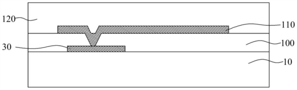
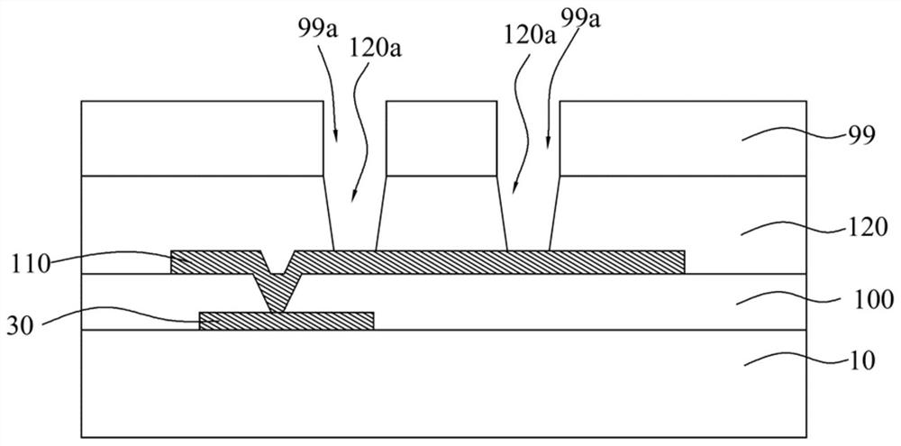
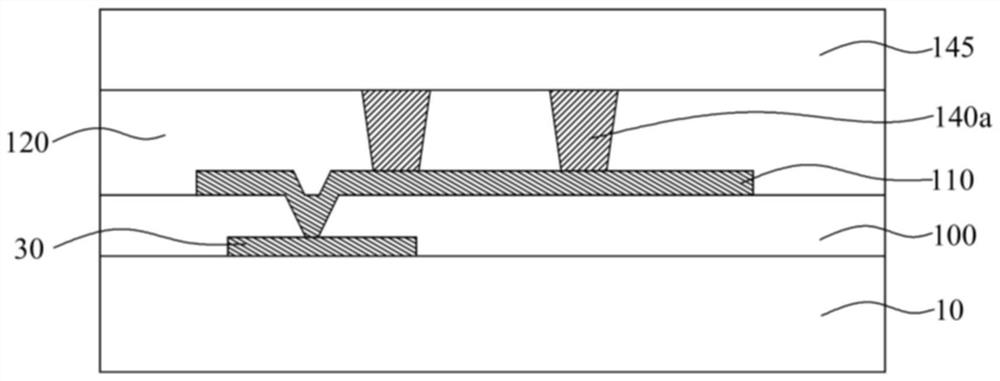
[0018] Please refer to Figure 1-9 , shows a schematic cross-sectional view of a method for manufacturing a metal probe structure according to an embodiment of the present invention.

[0019] Please refer to figure 1 First, a multilayer substrate 10 is provided, on which a first flexible dielectric layer 100 and a conductive layer 110 are sequentially formed, and a conductive layer 30 is formed between the multilayer substrate 10 and the flexible dielectric layer 100, It is ph...


PUM

PropertyMeasurementUnit
widthaaaaaaaaaa

Abstract

A metal probe structure and a method for fabricating the same are provided. The metal probe structure includes a multi-layer substrate, a first flexible dielectric layer, a second flexible dielectric layer, and a plurality of first metal components. The first flexible dielectric layer is disposed over the multi-layer substrate and has a conductive layer formed thereover. The second flexible dielectric layer is disposed over the first flexible dielectric layer to cover the conductive layer. The plurality of first metal components is disposed over the conductive layer and partially in the second flexible dielectric layer to serve as a metal probe.

Description

technical field [0001] The present invention relates to an integrated circuit test device, and in particular to a metal probe structure and a manufacturing method of a probe card for integrated circuit test. Background technique [0002] With the rapid development of the integrated circuit (Integrated Circuit) technology, the packaging technology has also reached an unprecedented and innovative technical level. [0003] The electrical testing of integrated circuits after packaging is mainly achieved by probe cards. According to the traditional technology, the measurement life of the test probes of the probe card will be affected by the ambient temperature, mechanical action and current resistance, and the test probes with a single structure cannot overcome the measurement errors caused by the above effects. [0004] In addition, when traditional test probes are used for wafer testing, the probe itself must have flexibility due to its compliance and the displacement it can w...

Claims


Application Information

Patent Timeline
Patent Type & Authority Applications(China)
IPC IPC(8): G01R1/067G01R3/00
CPCG01R1/06761G01R1/06733G01R3/00G01R1/07307G01R31/2886H05K1/0393H05K3/46G01R1/06716G03F7/422
Inventor 朱亦麟古鸿胜
Owner PRINCO CORP
Why Eureka
Try Eureka