Unlock instant, AI-driven research and patent intelligence for your innovation.

IGBT chip, manufacturing method thereof and power module

A manufacturing method and chip technology, applied to semiconductor devices, electrical components, resistors, etc., can solve problems such as overheating protection of IGBT chips

Active Publication Date: 2021-05-07
GREE ELECTRIC APPLIANCES INC +1
View PDF2 Cites 0 Cited by
  • Summary
  • Abstract
  • Description
  • Claims
  • Application Information

AI Technical Summary

Problems solved by technology

Some thermosensitive elements (NTC) are integrated on DBC (ceramic copper-clad substrate), and some are integrated in the internal circuit. There is a certain distance from the IGBT. The detected temperature has a certain deviation from the real temperature of the IGBT, which cannot Effectively protect the IGBT chip in the module from overheating

Method used


Image

  • IGBT chip, manufacturing method thereof and power module
  • IGBT chip, manufacturing method thereof and power module
  • IGBT chip, manufacturing method thereof and power module

Examples


Embodiment 1

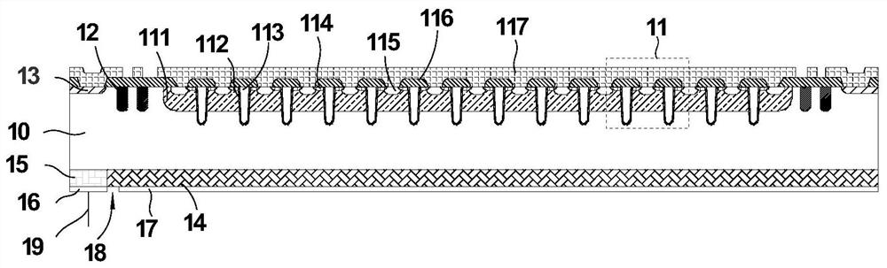
[0054] Such as figure 1 As shown, an IGBT chip includes:

[0055] substrate layer 10;

[0056]Several IGBT cells 11 disposed on the front side of the substrate layer 10 include a well region 111 , a gate oxide layer 112 , a gate 113 , a first source region 114 , a second source region 115 , an interlayer dielectric layer 116 and a front metal layer 11 .

[0057] The gates 113 are trench gates, which are located in a plurality of trenches etched downward from the upper surface of the substrate layer 10 , and the gates 113 are arranged in parallel.

[0058] The gate oxide layer 112 is located in the substrate layer 10 and covers the surface of the gate 113 .

[0059] The first source region 114 is located on the surface of the substrate layer 10 next to the gate 113 .

[0060] The second source region 115 is located on the surface of the substrate layer 10 and between two adjacent first source regions 114 , and has a depth greater than that of the first source region 114 .

...

Embodiment 2

[0077] An embodiment of the present disclosure provides a method for manufacturing an IGBT chip, which is used to manufacture the IGBT chip of Embodiment 1.

[0078] Below, refer to Figure 4 as well as Figure 5-Figure 8 An exemplary detailed step of the method for manufacturing an IGBT chip proposed by an embodiment of the present disclosure will be described.

[0079] Exemplarily, as Figure 4 Shown, the manufacturing method of the IGBT chip of the present embodiment comprises the following steps:

[0080] S101 : providing a substrate layer 10 , where a number of IGBT cells 11 are arranged on the front surface of the substrate layer 10 .

[0081] Specifically, the manufacturing method of the IGBT cell 11 includes: forming a well region 111 on the surface of the substrate layer 10 by ion implantation and diffusion; In preparation for preparation, the etching trench also separates the well region 111; the gate oxide layer 112 is filled in the etching trench, and the mater...

Embodiment 3

[0098] Such as Figure 8 and 9 As shown, the embodiment of the present disclosure provides a power module, including a fast recovery diode, a bootstrap diode, the IGBT chip of Embodiment 1, and a packaging wire frame structure. Wherein, the fast recovery diode and the bootstrap diode are respectively arranged in the package bonding frame structure and coupled to the IGBT chip.

[0099] In this embodiment, the design of the back side of the IGBT chip needs to match the frame of the module, and the module package wiring frame includes thermistor lead angle 301, IGBT wiring 302, FRD (fast recovery diode) wiring 303, IC wiring At 304, at 305 where the bootstrap diode is bonded, and at the lead angle 306. Corresponding to the backside design of the IGBT chip structure provided in Embodiment 1, the thermistor lead angle 301 is used to connect with the thermistor lead 19 on the backside of the IGBT chip.

[0100] A power module contains multiple ICs, multiple IGBT chips, where each ...


PUM


Abstract

The invention provides an IGBT chip, a manufacturing method thereof and a power module. The IGBT chip comprises a substrate layer, a plurality of IGBT cells arranged on the front surface of the substrate layer, and a collector layer arranged on the back surface of the substrate layer, wherein an etching groove is formed in the collector layer; the IGBT chip also comprises a thermistor which is arranged in the etching groove; the IGBT chip also comprises a first back metal layer which is arranged on the thermistor so as to be electrically connected with the thermistor. The thermistor is manufactured while the back face of the IGBT chip is manufactured, the thermistor is integrated on the back face of the IGBT chip and located on the same plane with the collector layer of the IGBT chip, then the metal layer on the back face of the thermistor and the metal layer on the back face of the collector layer are separated through an isolation groove, and the thermistor lead is independently led out, and is connected to an external control circuit, so that the real temperature of the IGBT chip can be tested, the IGBT chip can be better protected, and the working operation of the power module can be ensured.

Description

technical field [0001] The present disclosure relates to the technical field of semiconductor devices, in particular to an IGBT chip, its manufacturing method and a power module. Background technique [0002] Insulated Gate Bipolar Transistor (IGBT) is a composite fully-controlled voltage-driven power semiconductor device composed of BJT (Bipolar Transistor) and MOSFET (Metal Oxide Semiconductor Field Effect Transistor). The advantages of BJT and MOSFET have both the advantages of high impedance of MOSFET and the advantages of low conduction voltage drop of BJT. [0003] The power module is a switching device that integrates IGBT, FRD (fast recovery diode), bootstrap diode, DBC (ceramic copper-clad substrate) and drive circuit, and has built-in related protection circuit. It has high reliability, strong performance, and easy to use. Now industry, 4C (communication, computer, consumer electronics, automotive electronics), home appliances and other industries are widely used....

Claims


Application Information

Patent Timeline
IPC IPC(8): H01L29/06H01L29/739H01L49/02
CPCH01L29/0603H01L29/7393H01L28/20
Inventor 肖婷史波敖利波曾丹刘勇强
Owner GREE ELECTRIC APPLIANCES INC