Manufacturing method of high-precision rigid-flex circuit board
A combination of soft and hard, manufacturing method technology, applied in printed circuit manufacturing, multi-layer circuit manufacturing, printed circuit, etc., can solve the problems of non-solderability of conductive lines, large chemical plating solution, complex process, etc.
- Summary
- Abstract
- Description
- Claims
- Application Information
AI Technical Summary
Problems solved by technology
Method used
Image

Examples
Embodiment Construction
[0026] The following will clearly and completely describe the technical solutions in the embodiments of the present invention with reference to the accompanying drawings in the embodiments of the present invention. Obviously, the described embodiments are only some, not all, embodiments of the present invention. Based on the embodiments of the present invention, all other embodiments obtained by persons of ordinary skill in the art without making creative efforts belong to the protection scope of the present invention.
[0027] Below, in conjunction with accompanying drawing and specific embodiment, the present invention is further described:
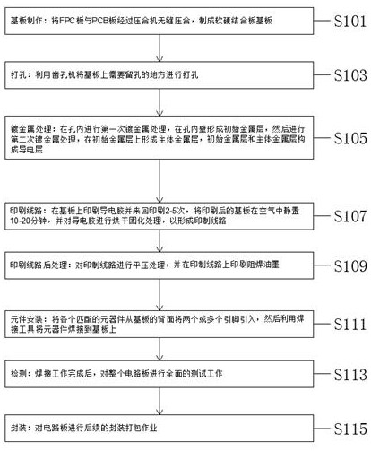
[0028] see figure 1 , according to a method for manufacturing a high-precision soft-rigid circuit board according to an embodiment of the present invention, the specific method is as follows:
[0029] S1: Substrate production: The FPC board and PCB board are seamlessly pressed together by a pressing machine to make a flexible and rigid...
PUM
| Property | Measurement | Unit |
|---|---|---|
| Thickness | aaaaa | aaaaa |
| Thickness | aaaaa | aaaaa |
Abstract
Description
Claims
Application Information
PatSnap Eureka turns technology decisions into work you can execute. Powered by our Innovation Knowledge Graph, it runs expert workflows across engineering, life sciences, materials and intellectual property. Get your review-ready output in minutes.


