Supercharge Your Innovation With Domain-Expert AI Agents!

Film forming apparatus and embedding processing apparatus

A film-forming device and processing unit technology, applied in ion implantation plating, vacuum evaporation plating, coating, etc., can solve problems such as film-forming position falling off, electronic parts upside down, etc.

Active Publication Date: 2021-05-14
SHIBAURA MECHATRONICS CORP
View PDF10 Cites 0 Cited by
  • Summary
  • Abstract
  • Description
  • Claims
  • Application Information

AI Technical Summary

Problems solved by technology

[0006] In the transportation of such electronic parts inside and outside the equipment, there is a possibility that the electronic parts may be turned upside down or fall off from the film-forming position due to inertial force received by the electronic parts due to acceleration, deceleration, rotation, etc.

Method used


Image

  • Film forming apparatus and embedding processing apparatus
  • Film forming apparatus and embedding processing apparatus
  • Film forming apparatus and embedding processing apparatus

Examples


Embodiment Construction

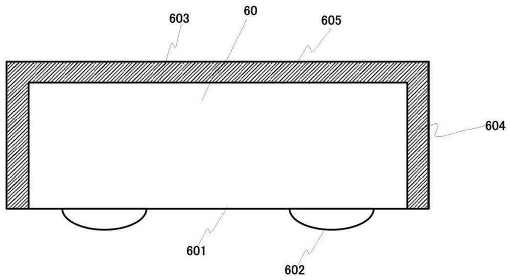
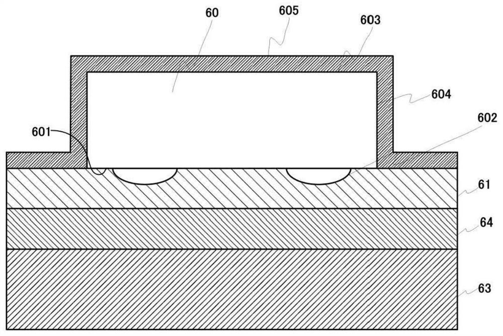
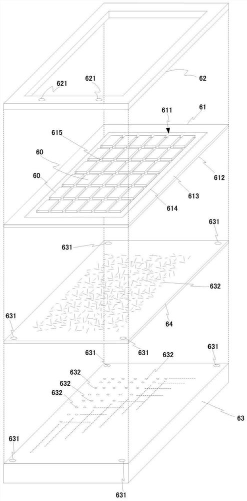
[0184] (electronic parts)

[0185] figure 1 It is a side view showing an electronic component subjected to film formation. Such as figure 1 As shown, an electromagnetic wave shielding film 605 is formed on the surface of the electronic component 60 . The electronic component 60 is a surface mount component such as a semiconductor chip, a diode, a transistor, a capacitor, or a surface acoustic wave (Surface Acoustic Wave, SAW) filter. A semiconductor chip is an integrated circuit (Integrated Circuit, IC) or a large scale integrated circuit (Large Scale Integrated circuit, LSI) and other integrated circuits formed by integrating multiple electronic components. This electronic component has ball grid array (Ball Grid Array, BGA), contact grid array (Land Grid Array, LGA), small outline package (Small Outline Package, SOP), quad flat package (Quad Flat Package, QFP), chip In a substantially rectangular parallelepiped shape such as a Wafer Level Package (WLP), one side become...


PUM

PropertyMeasurementUnit
lengthaaaaaaaaaa
diameteraaaaaaaaaa

Abstract

The invention provides a film forming apparatus, an embedding processing apparatus and a component peeling apparatus, which can prevent residues from remaining on an electronic component and peel the electronic component from a sheet. The electronic component, the electrode exposed surface of which has been adhered to the adhesive surface of the protective sheet, is put into a film forming apparatus. The film forming apparatus comprises a film forming processing part and a peeling processing part. The film-forming processing part forms a film on the electronic component with a film-forming material. The peeling processing part peels the electronic component from the protective sheet after the film formation by the film forming processing part. The peeling processing part is provided with the components: a carrying platform which supports the electronic component that has been pasted on the protective sheet; a chuck which holds an end portion of the protective sheet, moves relative to the mounting table, and continuously peels the protective sheet toward an end opposite to the end portion; and a fixing part for fixing the position of the electronic component.

Description

[0001] This application is a divisional application of the original application number 201811329890.5, the application date is November 09, 2018, and the invention name is "film forming device and part stripping device". technical field [0002] The present invention relates to a film forming device for forming a film on an electronic component pasted on a protective sheet, an embedding processing device, and a component peeling device for peeling the electronic component on which the film is formed from the protective sheet. Background technique [0003] Many electronic components such as semiconductor devices are mounted on wireless communication devices typified by mobile phones. Electronic components are conveyed from a processing device to a processing device in order to undergo various processes. As a representative example of processing, formation of an electromagnetic wave shielding film is mentioned. In order to prevent influence on communication characteristics, t...

Claims


Application Information

Patent Timeline
Patent Type & Authority Applications(China)
IPC IPC(8): C23C14/34
CPCC23C14/34C23C14/0005H01L21/67017H01L21/67103H01L21/67092H01L21/67132
Inventor 西垣寿铃木端生吉村浩司神戸优
Owner SHIBAURA MECHATRONICS CORP
Features
  • R&D
  • Intellectual Property
  • Life Sciences
  • Materials
  • Tech Scout
  • Unparalleled Data Quality
  • Higher Quality Content
  • 60% Fewer Hallucinations
Learn More