Method for increasing zinc doping concentration in indium phosphide

A technology of doping concentration and indium phosphide, which is applied in the direction of electrical components, semiconductor/solid-state device manufacturing, circuits, etc., can solve the problem that it is difficult to obtain P-type InP, etc., and achieve the goal of improving internal quantum efficiency, reducing thickness and manufacturing cost Effect

Active Publication Date: 2021-05-14
ZHONGSHAN DEHUA CHIP TECH CO LTD
View PDF6 Cites 0 Cited by
  • Summary
  • Abstract
  • Description
  • Claims
  • Application Information

AI Technical Summary

Problems solved by technology

[0004] Compared with other III-V materials, the diffusion coefficient of Zn in InP materials is larger, so it is difficult to obtain a P-type InP with a high doping concentration by conventional means. For example, the doping concentration of Zn in InGaAs can reach 10 19 cm -3 ~10 20 cm -3 , while the doping concentration of Zn in InP is generally 10 18 cm -3 , with a difference of about two orders of magnitude

Method used


Image

  • Method for increasing zinc doping concentration in indium phosphide
  • Method for increasing zinc doping concentration in indium phosphide
  • Method for increasing zinc doping concentration in indium phosphide

Examples


Embodiment 1

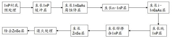
[0086] In this embodiment, a semi-finished infrared epitaxial wafer is prepared, and the specific process is as follows:

[0087] S1. Using Veeco K475 MOCVD, under the pressure of 39torr and temperature of 620℃, the surface pretreatment of InP substrate was carried out for 6min;

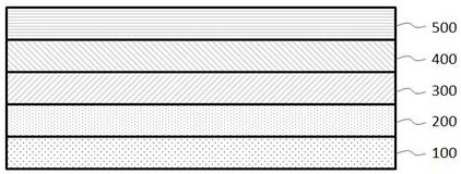
[0088]S2. Using the above-mentioned MOCVD instrument, grow a 0.5um thick InP buffer layer on the surface of the InP substrate at a temperature of 580°C, with a growth rate of 0.5um / h;

[0089] S3. Using the above-mentioned MOCVD instrument, grow a 0.2um thick InGaAs corrosion stop layer on the surface of the InP buffer layer at a temperature of 630°C, with a growth rate of 2.6um / h;

[0090] S4. Using the above-mentioned MOCVD instrument, grow a 0.1um thick n-InP layer on the surface of the InGaAs etching stop layer at a temperature of 580°C, with an n-type doping concentration of 4×10 18 cm -3 , the growth rate is 0.5um / h;

[0091] S5. Using the above-mentioned MOCVD instrument, grow a 2.5um thick...

Embodiment 2

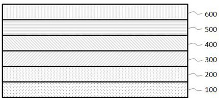
[0093] In this embodiment, an infrared epitaxial wafer comprising indium phosphide material with a high zinc doping concentration is prepared, and the specific process is as follows:

[0094] S1. Using the same MOCVD instrument as in Example 1, at a temperature of 580° C., on the surface of the i-InGaAs layer of the semi-finished infrared epitaxial wafer obtained in Example 1, grow a 0.2um thick p-InP layer. The average zinc (p type) with a doping concentration of 10 19 cm -3 , the growth rate is 0.5um / h; where the p-InP layer includes a 0.14um thick pure InP layer grown sequentially on the surface of the i-InGaAs layer, and a 0.06um thick zinc-doped InP layer; when growing a zinc-doped InP layer, The zinc source is dimethyl zinc, the zinc source feed time is 140s, and the feed rate is 30 sccm;

[0095] Using the above-mentioned MOCVD instrument, grow a 0.05um thick ZnSe layer on the surface of the p-InP layer at a temperature of 500°C, with a growth rate of 5um / h;

[0096]...


PUM

PropertyMeasurementUnit
thicknessaaaaaaaaaa
thicknessaaaaaaaaaa
thicknessaaaaaaaaaa

Abstract

The invention discloses a method for increasing the zinc doping concentration in indium phosphide, and belongs to the technical field of semiconductor materials. The method for increasing the zinc doping concentration in indium phosphide comprises the steps of: growing a ZnSe layer on the surface of indium phosphide subjected to zinc diffusion, then conducting annealing treatment, and removing the ZnSe layer. According to the ZnSe layer, in the annealing treatment process, Zni<m+> is prevented from escaping from an indium phosphide matrix, so that the probability that the Zni<m+> is activated and then converted into substitution site ZnS<-> is increased, and finally the zinc doping concentration in indium phosphide is increased.

Description

technical field [0001] The invention belongs to the technical field of semiconductors, and in particular relates to a method for increasing the zinc doping concentration in indium phosphide. Background technique [0002] Zinc (Zn) is a common p-type doping element in III-V materials, and has important applications in the fabrication of indium phosphide (InP)-based photodetectors and lasers. [0003] Some optoelectronic devices, such as photodetectors and avalanche photodetectors, need to precisely control the depth of Zn diffusion. However, the diffusion rate of Zn in III-V materials is very fast, and it is difficult to control the doping depth by means of epitaxial doping. Depth of Zn. The metal-organic chemical vapor deposition (MOCVD) method has the advantages of good temperature uniformity, good arsenic and phosphorus overvoltage protection, and high precision control of impurity concentration. It can obtain devices with excellent performance and improve the yield of de...

Claims


Application Information

Patent Timeline
Patent Type & Authority Applications(China)
IPC IPC(8): H01L21/22H01L21/02H01L21/324
CPCH01L21/02568H01L21/2225H01L21/3245
Inventor 黄辉廉黄珊珊张小宾黄彦泽杨文奕
Owner ZHONGSHAN DEHUA CHIP TECH CO LTD
Why Eureka
Try Eureka