Solar cell and preparation method thereof

A solar cell and metal electrode technology, applied in the field of solar power generation, can solve the problems of reducing the short-circuit current of the battery, difficulty in taking into account the light absorption and passivation effect of the battery, and the strong light absorption coefficient, etc.

Pending Publication Date: 2021-05-18
CSI CELLS CO LTD +1
View PDF0 Cites 6 Cited by
  • Summary
  • Abstract
  • Description
  • Claims
  • Application Information

AI Technical Summary

Problems solved by technology

However, the polysilicon film layer in the above-mentioned passivation structure has a strong light absorption coefficient, so it will reduce the short-circuit current of the battery, thereby limiting the improvement of battery efficiency
At present, the current loss is mainly reduced by reducing the thickness of the polysilicon film layer as much as possible under the premise of ensuring that the metal electrode paste does not burn through the tunneling oxide layer and the metal electrode forms a good ohmic contact with the polysilicon film layer; or only in the battery The above-mentioned passivation structure is used in the metal electrode area of ​​the battery, and it is difficult to balance the light absorption and passivation effects of the battery
It is also disclosed in the industry that the polysilicon doped layer on the tunneling layer is arranged in the first area and the second area with different thicknesses, and the metal electrode is located on the first area with a larger thickness, but the preparation process of the polysilicon doped layer with different thicknesses is relatively complex. Complicated; and as the overall thickness of the film layer decreases, it is more difficult to differentiate the thickness of different regions of the above-mentioned polysilicon doped layer

Method used


Image

  • Solar cell and preparation method thereof
  • Solar cell and preparation method thereof
  • Solar cell and preparation method thereof

Examples


Embodiment Construction

[0033] The present application will be described in detail below in conjunction with the implementations shown in the accompanying drawings. However, this embodiment does not limit the present application, and any structural, method, or functional changes made by those skilled in the art according to this embodiment are included in the protection scope of the present application.

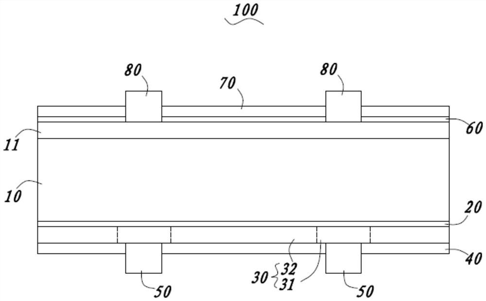
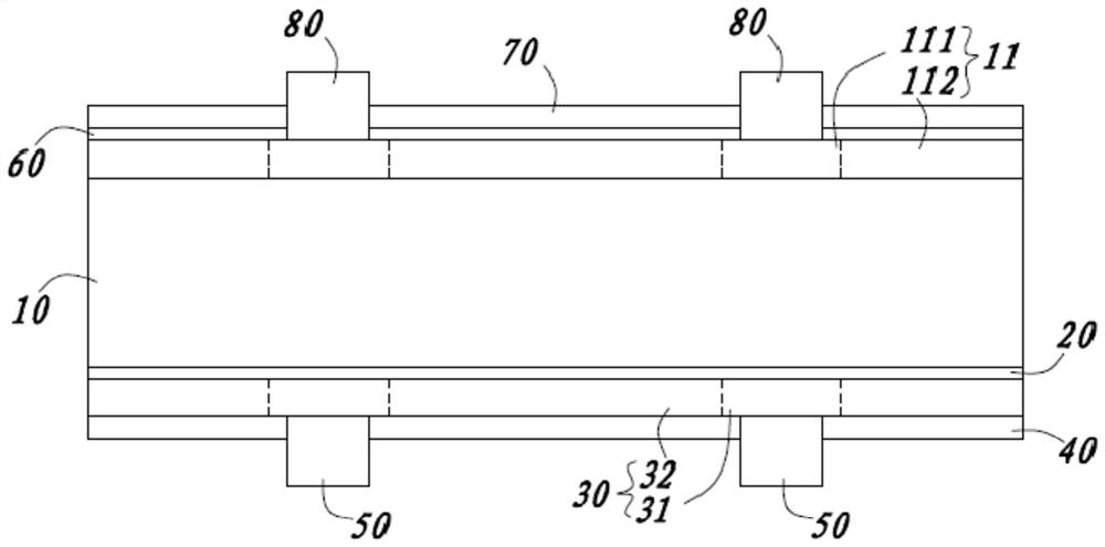
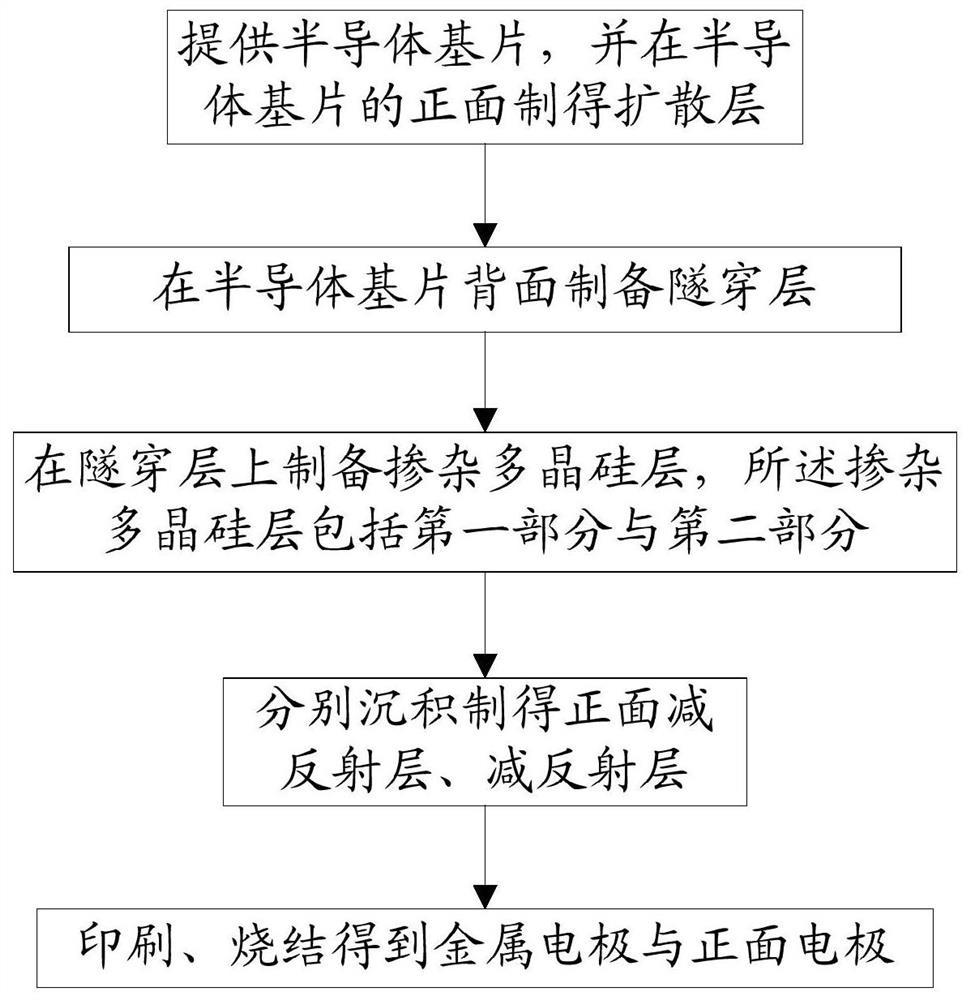
[0034] ginseng figure 1 As shown, the solar cell 100 provided in this application includes a semiconductor substrate 10, a tunneling layer 20 stacked on one side of the semiconductor substrate 10, a doped polysilicon layer 30, an anti-reflection layer 40, and a layer penetrating through the semiconductor substrate 10. The anti-reflection layer 40 and the metal electrode 50 in contact with the doped polysilicon layer 30 .

[0035] The tunneling layer 20 can isolate the contact between the metal electrode 50 and the semiconductor substrate 10 without affecting the current transfer. It is combined wit...


PUM

PropertyMeasurementUnit
thicknessaaaaaaaaaa
thicknessaaaaaaaaaa
thicknessaaaaaaaaaa

Abstract

The invention provides a solar cell and a preparation method thereof, the solar cell comprises a semiconductor substrate, a metal electrode, and a tunneling layer, a doped polycrystalline silicon layer and an antireflection layer which are sequentially stacked on the surface of one side of the semiconductor substrate, the doped polycrystalline silicon layer is provided with a first part and a second part, the doping concentration of the first part is greater than that of the second part, and the metal electrode penetrates through the antireflection layer and is in contact with the first part. The preparation of the doped polycrystalline silicon layer is simpler, the first part with higher doping concentration is obtained through local doping, and the interface recombination and contact resistance at the position of a metal electrode are effectively reduced; and due to the fact that the doping concentration of the second part is low, the non-electrode area is passivated, and meanwhile light absorption is reduced.

Description

technical field [0001] The present application relates to the technical field of solar power generation, in particular to a solar cell and a preparation method thereof. Background technique [0002] With the rapid development of photovoltaic technology, the market demand for high-efficiency cells and modules is also increasing. As far as the crystalline silicon battery is concerned, a passivation anti-reflection layer is often provided on the front side, and the front electrode penetrates the passivation anti-reflection layer to contact the silicon substrate; a kind of partial contact back passivation battery has also been disclosed in the industry, that is, through the back passivation The chemical film reduces the recombination of surface carriers and improves the conversion efficiency of the battery. [0003] The industry also discloses a passivation structure combining a tunnel oxide layer and a polysilicon film layer, which can reduce the recombination loss caused by t...

Claims


Application Information

Patent Timeline
Patent Type & Authority Applications(China)
IPC IPC(8): H01L31/068H01L31/0216H01L31/0288H01L31/18
CPCH01L31/02168H01L31/0288H01L31/068H01L31/182Y02E10/546Y02P70/50
Inventor 李兵邓伟伟
Owner CSI CELLS CO LTD
Why Eureka
Try Eureka