
Photoelectric detection unit, photoelectric detection structure, photoelectric detector and preparation method thereof
A technology of photoelectric detection and isolation structure, which is applied in the field of photoelectric detection, can solve the problem that the detection accuracy of the photoelectric detection structure is difficult to improve, and achieve the effect of improving light absorption efficiency and increasing the propagation optical path
- Summary
- Abstract
- Description
- Claims
- Application Information
AI Technical Summary
Problems solved by technology
Method used
Image

Examples
no. 1 example
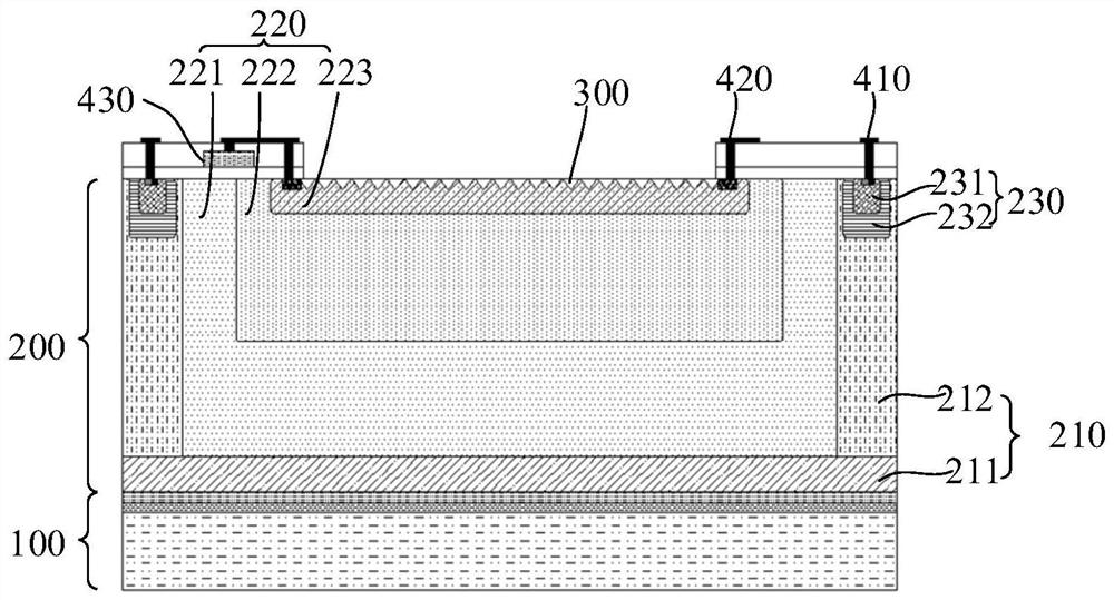
[0056] Such as figure 1 Shown is a schematic structural diagram of the photodetection unit in the first embodiment.
[0057]The photodetection unit includes a first substrate 100 and a photodetection layer 200 formed on the first substrate 100 . The photodetection layer 200 specifically includes a first structure 210 disposed on the first substrate 100 , and a second structure 220 formed in the first structure 210 . Wherein, the side surface and the bottom surface of the second structure 220 are wrapped by the first structure 210, and the top surface of the second structure 220 is not in contact with the first structure 210, that is, the first structure 210 has a bottom wall 211 in contact with the bottom surface of the second structure 220 and The sidewall 212 is in side contact with the second structure 220 .
[0058] The first photoprocessing layer 300 is disposed on the second structure 220, and the surface of the first photoprocessing layer 300 has a concave-convex stru...
no. 2 example
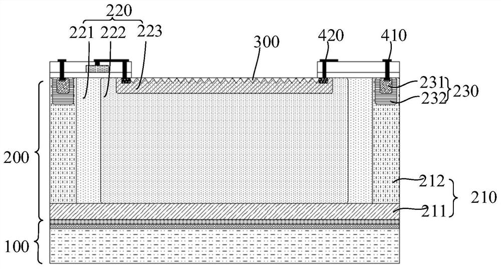
[0073] Such as figure 2 Shown is a schematic structural diagram of the photodetection unit in the second embodiment.
[0074] The difference between the second embodiment and the first embodiment is that, in the second embodiment, the bottom of the second doped region 222 extends to the bottom wall 211 and is in contact with the bottom wall 211, that is, the second doped region 222 runs through the first The doped region 221 is in contact with the bottom wall 211 , the first doped region 221 covers the side surface of the second doped region 222 , and the bottom wall 211 covers the bottom surface of the second doped region 222 .
no. 3 example
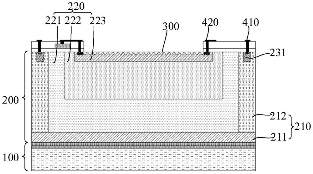
[0076] Such as image 3 Shown is a schematic structural diagram of the photodetection unit in the third embodiment.
[0077] The difference between the third embodiment and the first embodiment is that, in the third embodiment, the heavily doped region 230 may only include the first heavily doped region 231 .
PUM
 Abstract
Description
Claims
Application Information