Manufacturing method of stress adjusting micron LED chip

A LED chip and stress adjustment technology, applied in the field of micro-LEDs, can solve problems such as uneven current distribution of LED chips, limited improvement effect, and immature micro-LED technology, so as to avoid surface non-radiative radiation effects and serious current uniformity , to avoid the effect of the polarization effect is not obvious

Inactive Publication Date: 2021-06-04
YANCHENG TEACHERS UNIV
View PDF3 Cites 0 Cited by
  • Summary
  • Abstract
  • Description
  • Claims
  • Application Information

AI Technical Summary

Problems solved by technology

[0002] The lattice mismatch between the substrate of the LED chip and the PN junction material, and the area of ​​the ordinary-sized LED chip is relatively large, so the substrate of the LED chip and the PN junction material generate a lot of stress, and this stress will occur in the active area of ​​the LED chip. A large polarization effect is generated, resulting in uneven current distribution of the LED chip, and these all help to improve the light output efficiency of the LED chip. The existing micro-LED technology is not mature enough. Due to the small size of the micro-LED, the micro-LED The stress release is obvious, and the stress generated by the substrate of the micro-LED chip and the PN junction material is very small compared with the stress of the ordinary LED chip, so the polarization effect of the active area of ​​the micro-LED chip is not obvious, which makes the current of the micro-LED chip very uniform , and these greatly reduce the light extraction efficiency of the micron LED
Existing micro-LEDs lack a method for fabricating micro-LEDs that can generate stress
[0003] In addition, the surface area to volume ratio of micron LED chips is much larger than that of ordinary micron LED chips, and the damage caused by the sidewall etching of existing micron LED chips is relatively serious. This loss will be due to the larger surface area to volume ratio of micron LED chips And larger, because the proportion of surface effect will be larger, which will cause serious non-radiative recombination of the existing micro-LED carriers on the side surface, which will seriously reduce the light extraction efficiency of the existing micro-LED. The existing method can be passed Post-processing to improve, the improvement effect is limited and cannot completely solve this problem, the existing micro LED chip lacks a manufacturing method that fundamentally solves the low light extraction efficiency caused by side surface damage
[0004] The existing stress-regulating micro-LED chip stress-regulating components and the intermediate semiconductor material are transparent under visible light. How to ensure that the stress-regulating component and the surrounding semiconductor material can be distinguished during lithography is not possible with existing lithography equipment. The problem to be solved, the existing LED manufacturing method lacks a manufacturing method that ordinary lithography cannot distinguish between the stress adjustment component and the intermediate semiconductor material processing technology
[0005] Aiming at the deficiencies of the existing technology, those skilled in the art invented a method for manufacturing stress-regulated micro-LED chips to solve the problem of uniform stress distribution of micro-LEDs and non-radiative recombination effects caused by sidewall damage, and improve the performance of micro-LED chips. Light efficiency

Method used


Image

  • Manufacturing method of stress adjusting micron LED chip
  • Manufacturing method of stress adjusting micron LED chip
  • Manufacturing method of stress adjusting micron LED chip

Examples


Embodiment Construction

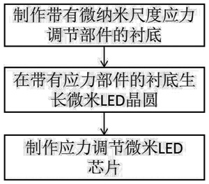
[0031] In order to better understand the purpose and function of the present invention, a method for manufacturing stress-regulated micro-LED chips of the present invention will be further described in detail below in conjunction with the accompanying drawings.

[0032] according to figure 1 , a method for manufacturing a stress-regulated micro-LED chip according to an embodiment of the present invention includes:

[0033] Step 111: Fabricate the substrate 1 with the micro-nano scale stress adjustment component 3;

[0034] Step 112: growing micro-LED wafers on the substrate with stress components;

[0035] Step 113: Fabricate stress-regulated micro-LED chips.
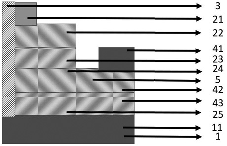
[0036] Furthermore, the area of ​​the micro-nano-scale stress adjustment component 3 is less than or equal to 50000µm 2 ; The production process of the micro-nano scale stress adjustment component 3 includes:

[0037] Step 1111: Depositing a stress-adjusting material on the substrate;

[0038] Step 1112:

[0039] ...


PUM

PropertyMeasurementUnit
areaaaaaaaaaaa

Abstract

The invention provides a manufacturing method of a stress adjusting micron LED chip, and belongs to the technical field of micron LEDs. The method comprises the steps of manufacturing a substrate with a micro-nano scale stress adjusting component, growing a micron LED wafer on the substrate with the stress component, and manufacturing the stress adjusting micron LED chip. According to the manufacturing method of the stress adjusting micron LED chip, stress, polarization and uneven distribution of current are generated on a PN junction area through the stress adjusting component, the light emitting efficiency of the micro LED is improved, meanwhile, an insulating stress adjusting component etching area is added to replace a semiconductor material etching area of the micro LED chip, the surface non-radiation effect caused by side wall damage is avoided, the light extraction efficiency of the micron LED chip is improved, meanwhile, photoetching is carried out through ultraviolet imaging equipment, the problem that production cannot be carried out through existing common photoetching is solved, and the micron LED chip has the advantages of being extremely high in innovativeness, capable of saving energy, environmentally friendly, simple in structure and the like and has the extremely high application market.

Description

technical field [0001] The invention relates to a technology for manufacturing micro-LEDs, in particular to a method for manufacturing stress-regulated micro-LED chips, which belongs to the technical field of micro-LEDs. Background technique [0002] The lattice mismatch between the substrate of the LED chip and the PN junction material, and the area of ​​the ordinary-sized LED chip is relatively large, so the substrate of the LED chip and the PN junction material generate a lot of stress, and this stress will occur in the active area of ​​the LED chip. A large polarization effect is generated, resulting in uneven current distribution of the LED chip, and these all help to improve the light output efficiency of the LED chip. The existing micro-LED technology is not mature enough. Due to the small size of the micro-LED, the micro-LED The stress release is obvious, and the stress generated by the substrate of the micro-LED chip and the PN junction material is very small compar...

Claims


Application Information

Patent Timeline
Patent Type & Authority Applications(China)
IPC IPC(8): H01L33/00H01L33/14
CPCH01L33/005H01L33/14
Inventor 魏伟苗中正封然
Owner YANCHENG TEACHERS UNIV
Why Eureka
Try Eureka