[0076] In order to describe in detail the technical content, achieved objects and effects of the present invention, the following descriptions are given with reference to the embodiments and the accompanying drawings. The test methods used in the examples are conventional methods unless otherwise specified; the materials, reagents, etc. used, unless otherwise specified, can be obtained from commercial sources.
[0077] The embodiments of the present invention are: a flexible planar detector PIN chip and a preparation method thereof, comprising the following steps:
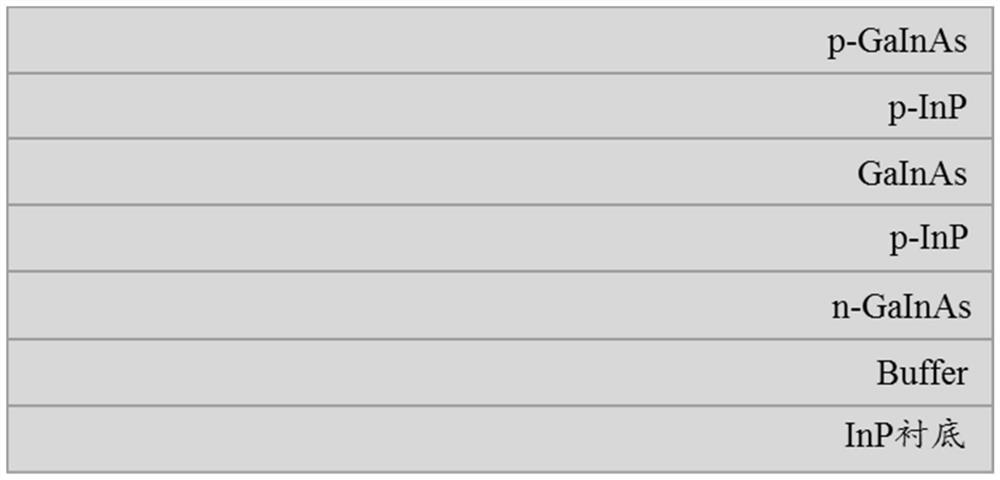
[0078] S1. A Buffer layer (InP) is grown on the surface of the InP substrate, and the following layers are grown in sequence from the Buffer layer by MOCVD method: n-type InGaAs ohmic contact layer, n-type InP layer, InGaAs layer, p-type InP layer and p-type InGaAs ohmic contact layer, prepared as figure 1 A preform A shown;
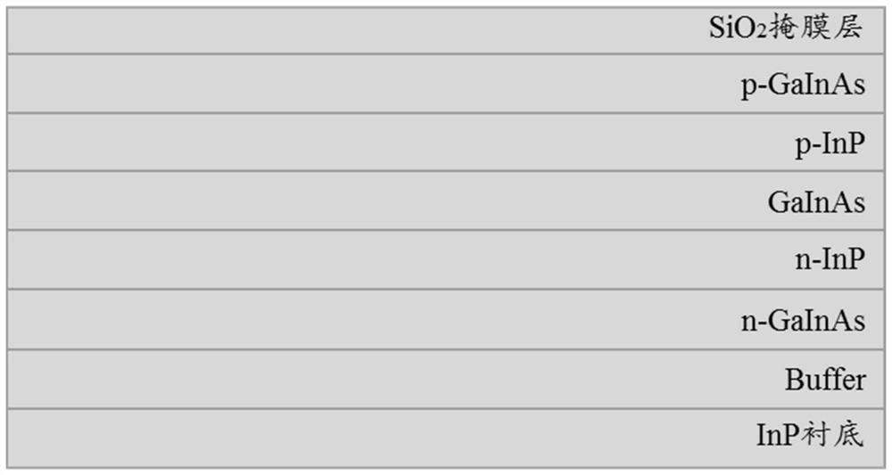
[0079] S2. Deposit SiO on the surface of the p-type InGaAs ohmic contact layer of preform A 2 mask layer, made as figure 2 The shown preform B; wherein, the deposition method is plasma enhanced chemical vapor deposition;
[0080] S3, prefabricate the SiO in B 2 After photolithography in a specific area of the mask layer, an aqueous solution of HF with a mass fraction of 10% is used for etching to form a contact ring mask; 3 PO 4 and H 2 O 2 The mixed solution (wherein, the mass ratio of water: phosphoric acid: hydrogen peroxide is 1: 1: 0.2) is etched to the P-type InGaAs ohmic contact layer to form a P-type InGaAs ohmic contact ring. image 3 Shown as prefab C; wherein the P-type InGaAs ohmic contact ring is the same size as the contact ring mask;
[0081] S4, depositing SiO on the opposite side of the preform C and the InP substrate 2 insulating layer, made as Figure 4 Prefab D shown;
[0082] S5, the surface SiO of the prefabricated D 2 Partial area of insulating layer and SiO 2 After the photolithography of the mask layer, an aqueous solution of 10% HF was selected for etching, and the diffusion hole area was exposed. Figure 5 The shown preform E; wherein, the diffusion hole area includes a P-type InGaAs ohmic contact ring and an inner area of the ring;
[0083] S6. Diffusion of Zn is carried out on the prefab E by MOCVD method. After the diffusion is completed, anneal at 550° C. for 1 min to obtain the following Image 6 Preform F shown; where the diffusion source is dimethylzinc (DMZn) and PH 3 Zinc phosphide formed at high temperature;
[0084] S7, deposit a SiNx anti-reflection film on the upper surface of the preform F to obtain the following Figure 7 The preform G shown; wherein, the deposition method is plasma enhanced chemical vapor deposition;
[0085] S8, etch the prefab G after lithography, and expose the P-type InGaAs ohmic contact ring to obtain the following Figure 8 The shown prefab H; wherein, the etching process uses inductively coupled plasma for etching and wet etching with a mass fraction of 10% HF aqueous solution;
[0086] S9, sputtering a P-surface electrode on the surface of the P-type InGaAs ohmic contact ring of the prefabricated H, after the sputtering is completed, attach a pyrolysis adhesive film to the upper surface, and attach a silicon wafer to the surface of the pyrolysis adhesive film to obtain the following Figure 9 The preform I shown; wherein, the P-surface electrode structure is a Ti layer, a Pt layer and an Au layer; the thickness of the Ti layer in the P-surface electrode is 50 nm, the thickness of the Pt layer is 100 nm, and the thickness of the Au layer is 1000 nm; P The sputtering method of the surface electrode is a magnetron sputtering coating method; the pyrolysis adhesive film is a double-sided adhesive film;
[0087] S10, use the aqueous solution of HCl to etch the InP substrate and the Buffer layer of the prefab I, and expose the InGaAs ohmic contact layer to obtain the following Figure 10 Pre-production J shown;
[0088] S11. Prepare an N-surface electrode on the surface of the InGaAs ohmic contact layer of the prefabricated J, and electroplate a copper substrate on the surface of the N-surface electrode to obtain the following Figure 11 The preform K shown; wherein, the N-face electrode structure is Ni layer, Ge layer, Au layer, Ti layer and Cu layer; wherein, the thickness of the N-face electrode Ni layer is 10nm, the thickness of Ge layer is 100nm, and the thickness of Au layer is 10 nm. The thickness of the layer is 100 nm, the thickness of the Ti layer is 100 nm, and the thickness of the Cu layer is 1000 nm; wherein, the preparation method of the N-surface electrode is the electron beam evaporation coating method; wherein, the electroplating solution is CuSO with a mass fraction of 20% 4 and a mass fraction of 6.5% H 2 SO 4 Mixed solution, the thickness of electroplated copper substrate is 40μm;
[0089] S12, heating the prefab K to remove the pyrolytic adhesive film and the silicon wafer, wherein the temperature for removing the pyrolytic adhesive film and the silicon wafer is 200°C, and the peeled epitaxial layer is annealed at a low temperature to obtain the following Figure 12 The flexible planar detector PIN chip shown; the low-temperature annealing temperature is 200°C, and the low-temperature annealing time is 90min.
[0090] To sum up, the preparation method provided by the present invention obtains a flexible planar detector PIN chip, and the application scenarios are not limited to conventional packaging forms, and can be used in complex environments such as various curved surfaces and flexible devices.
[0091] The above descriptions are only examples of the present invention, and are not intended to limit the scope of the patent of the present invention. Any equivalent transformations made by using the contents of the description and drawings of the present invention, or directly or indirectly applied in related technical fields, are similarly included in the within the scope of patent protection of the present invention.