Wafer cleaning fixing device

A technology for fixing devices and wafers, which is applied in cleaning methods and utensils, semiconductor/solid-state device manufacturing, electrical components, etc. The effect of excessive clamping force, reducing cleaning burden and improving production quality

Pending Publication Date: 2021-06-15
昆山基侑电子科技有限公司
View PDF0 Cites 2 Cited by
  • Summary
  • Abstract
  • Description
  • Claims
  • Application Information

AI Technical Summary

Problems solved by technology

[0002] Wafer refers to the silicon wafer used in the production of silicon semiconductor integrated circuits. Because of its circular shape, it is called a wafer. It can be processed into various circuit element structures on the silicon wafer and become an IC with specific electrical functions. Products, the raw material of the wafer is silicon, and the surface of the earth's crust is inexhaustible silicon dioxide, the silicon dioxide ore is refined by an electric arc furnace, chlorinated with hydrochloric acid, and distilled to produce a high-purity polysilicon wafer. The factory melts the polysilicon again, and then plants a seed crystal in the melt, and then slowly pulls it out to form a cylindrical single crystal silicon rod, because the silicon crystal rod is a seed determined by a crystal plane orientation. Crystals are gradually formed in molten silicon raw materials. This process is called "grown crystals". After the silicon crystal rods are cut into sections, rolled, sliced, chamfered, polished, laser engraved, and packaged, they become integrated circuit factories. The basic raw material of silicon wafers, this is the "wafer". During the processing of the wafer, the wafer needs to be cleaned, so a special fixing device is needed. The existing fixing devices mostly use fixed-size The mold is used to fix the wafer, and a large number of fixed molds need to be reserved. During the cleaning process of the wafer, the wafer needs to be taken out and turned over, and then cleaned. There are many shortcomings, and it is not suitable for clamping and fixing wafers of different diameters. The scope of application is small, the clamping force is too large, it is easy to damage the wafer, it is not convenient to turn the wafer over, the cleaning efficiency of the wafer is low, the limit effect of the device is poor, and the position of the wafer is prone to shift during the cleaning process, which cannot be guaranteed cleaning quality of the device, therefore a wafer cleaning fixture is proposed

Method used


Image

  • Wafer cleaning fixing device

Examples


Embodiment Construction

[0019] The technical solutions in the embodiments of the present invention will be clearly and completely described below in conjunction with the accompanying drawings in the embodiments of the present invention. Obviously, the described embodiments are only some of the embodiments of the present invention, not all of them. Based on The embodiments of the present invention and all other embodiments obtained by persons of ordinary skill in the art without making creative efforts belong to the protection scope of the present invention.

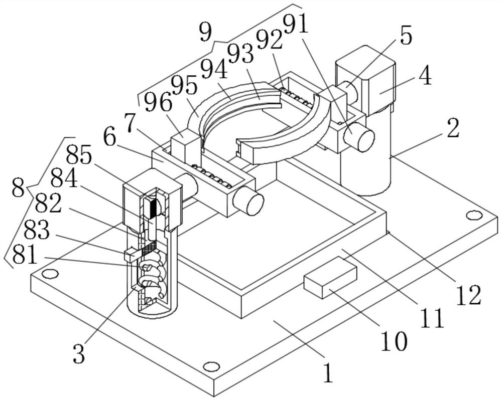
[0020] see figure 1 , the present invention provides a technical solution: a wafer cleaning and fixing device, including a bottom plate 1, a limiting mechanism 8 and a fixing mechanism 9;

[0021] Bottom plate 1: Hollow columns 2 are provided at the left and right ends of the upper surface. Bottom plate 1 provides support connection and installation and fixing places. Hollow column 2 provides stable support. 3 provide sliding support, the upper...


PUM


Abstract

The invention discloses a wafer cleaning and fixing device which comprises a bottom plate, limiting mechanisms and fixing mechanisms. wherein hollow columns are arranged at the left end and the right end of the upper surface of the bottom plate, rectangular openings are formed in the middle of the outer arc surfaces of the hollow columns, hollow blocks are arranged on the upper end surfaces of the hollow columns, rotating columns are rotationally connected to the opposite inner side surfaces of the two hollow blocks through bearings, supporting plates are arranged at the opposite inner side ends of the two rotating columns, and strip-shaped openings are formed in the middle of the supporting plates; the limiting mechanisms are arranged in the hollow columns correspondingly, the upper ends of the limiting mechanisms are fixedly connected with the outer side ends of the rotating columns on the same sides correspondingly, and the middle parts of the limiting mechanisms are slidably connected with the rectangular openings on the same sides correspondingly; and the fixing mechanisms are arranged on the front end faces of the supporting plates correspondingly, and the rear ends of the fixing mechanisms are slidably connected with the strip-shaped openings in the same sides correspondingly. The wafer cleaning fixing device is suitable for clamping and fixing wafers with different diameters, the wafers can be turned over conveniently, and the cleaning quality of the device can be guaranteed.

Description

technical field [0001] The invention relates to the technical field of wafer processing, in particular to a wafer cleaning and fixing device. Background technique [0002] Wafer refers to the silicon wafer used in the production of silicon semiconductor integrated circuits. Because of its circular shape, it is called a wafer. It can be processed into various circuit element structures on the silicon wafer and become an IC with specific electrical functions. Products, the raw material of the wafer is silicon, and the surface of the earth's crust is inexhaustible silicon dioxide, the silicon dioxide ore is refined by an electric arc furnace, chlorinated with hydrochloric acid, and distilled to produce a high-purity polysilicon wafer. The factory melts the polysilicon again, and then plants a seed crystal in the melt, and then slowly pulls it out to form a cylindrical single crystal silicon rod, because the silicon crystal rod is a seed determined by a crystal plane orientation...

Claims


Application Information

Patent Timeline
Patent Type & Authority Applications(China)
IPC IPC(8): H01L21/687H01L21/67B08B13/00
CPCB08B13/00H01L21/6704H01L21/68721
Inventor 周志刚王静强徐福兴黄锡钦陈亮
Owner 昆山基侑电子科技有限公司
Why Eureka
Try Eureka