A cyanide-free chemical gold plating solution and its gold plating process applied in the field of wafer advanced packaging

A technology in the field of chemical gold plating, which is applied in the field of cyanide-free chemical gold plating solution and its gold plating process, and can solve problems such as voids, inability to achieve the effect of uniform plating, cracks, etc.

Active Publication Date: 2021-09-10
SHENZHEN CHENGGONG CHEM
View PDF4 Cites 0 Cited by
  • Summary
  • Abstract
  • Description
  • Claims
  • Application Information

AI Technical Summary

Problems solved by technology

The earliest electroless gold plating used cyanide-containing gold salts as raw materials. Due to the highly toxic cyanide contained in the cyanide plating solution, there will be great unsafe factors in the actual production process and related follow-up wastewater, waste gas treatment and disposal. The development of cyanide gold plating solution is limited. With the improvement of people's awareness of environmental protection, more and more cyanide-free gold plating processes are now used in the process, but the existing cyanide-free gold plating process also has the following defects:
[0005] 1) Gold plating is prone to defects such as voids and cracks during electroplating, and it is impossible to achieve perfect and seamless electroplating filling, and it is still impossible to achieve the effect of uniform plating
[0006] 2) There is a certain gap between the current efficiency and stability of the existing plating solution, the corrosion resistance of the coating and the brightness of the appearance and the cyanide coating

Method used


Image

  • A cyanide-free chemical gold plating solution and its gold plating process applied in the field of wafer advanced packaging
  • A cyanide-free chemical gold plating solution and its gold plating process applied in the field of wafer advanced packaging
  • A cyanide-free chemical gold plating solution and its gold plating process applied in the field of wafer advanced packaging

Examples


Embodiment 1

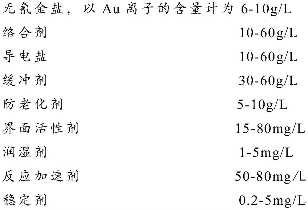
[0060] A kind of cyanide-free chemical gold-plating solution, every 1 liter of described cyanide-free chemical gold-plating solution comprises following composition:

[0061]

[0062] Adjust the pH to 7.2 with sulfuric acid or potassium hydroxide;

[0063] The balance is water.

[0064] Operating temperature: 50°C.

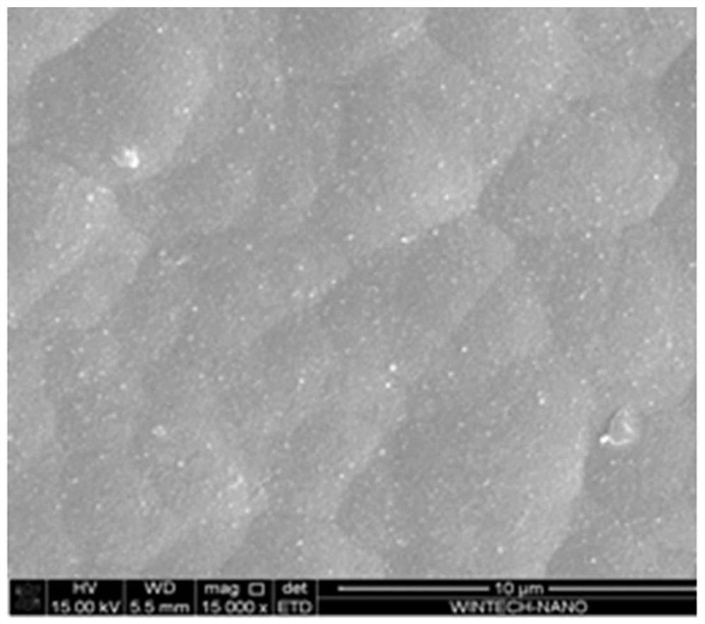
[0065] Using the gold-plating solution prepared by this component, after using the gold-plating method to carry out cyanide-free gold-plating on wafer packaging products, the thickness of the gold finally obtained is 0.3 microns; using the solution and gold-plating process of the present invention, the whole process only needs 20 minutes to complete ; And the crystal size of the obtained gold-plated layer is consistent, without voids and cracks; the surface is smooth.

Embodiment 2

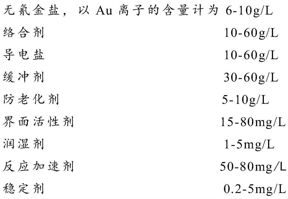
[0067] A kind of cyanide-free chemical gold immersion solution, every 1 liter of described cyanide-free chemical gold immersion solution comprises following composition:

[0068]

[0069] Adjust the pH to 8 with sulfuric acid or potassium hydroxide;

[0070] The balance is water.

[0071] Operating temperature: 60°C.

[0072] Using the gold plating solution prepared by this component, after using the gold plating method to carry out cyanide-free gold plating on wafer packaging products, the gold thickness is 0.2 microns; using the solution and gold plating process of the present invention, the whole process only needs 12 minutes to complete; and obtained The crystallization of the gold-plated layer is consistent in size, without voids or cracks; the surface is smooth.

Embodiment 3

[0074]

[0075]

[0076] Adjust the pH to 9 with sulfuric acid or potassium hydroxide;

[0077] The balance is water.

[0078] Operating temperature: 80°C.

[0079] Using the gold plating solution prepared by this component, after using the gold plating method to carry out cyanide-free gold plating on wafer packaging products, the gold thickness is 0.05 microns; using the solution and gold plating process of the present invention, the whole process only needs 2 minutes to complete; and obtained The crystallization of the gold-plated layer is consistent in size, without voids or cracks; the surface is smooth.


PUM


Abstract

The invention discloses a cyanide-free chemical gold-plating solution and a gold-plating process applied to the field of advanced packaging of wafers. 10-60g / L; conductive salt 10-60g / L; buffer 30-60g / L; anti-aging agent 5-10g / L; surfactant 15-80mg / L; wetting agent 1-5mg / L; reaction Accelerator 50-80mg / L; Stabilizer 0.2-5mg / L; The reaction accelerator is a compound of 2,6-diaminopyridine and 3-pyridinemethanol, and 2,6-diaminopyridine and 3-pyridine The mass concentration ratio of methanol is 2:1. The solution obtained by the invention not only ensures the stability of the plating solution, but also makes it easy to spread the plated parts on the surface of the electrode to achieve the purpose of uniform plating, and further achieves the effect of filling the micropores of the wafer package without voids and gaps.

Description

technical field [0001] The invention relates to the technical field of surface treatment, in particular to a cyanide-free chemical gold plating solution and a gold plating process applied in the field of advanced wafer packaging. Background technique [0002] The general orientation of wafer-level packaging is to perform most or all of the packaging and testing procedures directly on the wafer, and then cut it into a single component. Wafer-level packaging has a smaller package size and better electrical performance. At present, it is mainly used in various semiconductor products, and its demand mainly comes from the requirements of portable products for light, thin and small features. [0003] In the production process of wafer-level packaging products, when the copper lines are formed, other metals need to be formed on the copper lines to protect the copper lines and prevent oxidation. In addition, functions such as wire bonding and welding can be realized to form intercon...

Claims


Application Information

Patent Timeline
Patent Type & Authority Patents(China)
IPC IPC(8): C25D3/48C25D7/12C25D21/12
CPCC25D3/48C25D7/12C25D21/12
Inventor 洪学平姚吉豪
Owner SHENZHEN CHENGGONG CHEM
Why Eureka
Try Eureka