Cyanide-free chemical gold plating solution applied to advanced wafer packaging field and gold plating process thereof
A technology in the field of chemical gold plating, applied in the field of cyanide-free chemical gold plating solution and its gold plating process, can solve the problems of the development limitation of cyanide gold plating solution, the inability to achieve the effect of uniform plating, and the inability to achieve electroplating filling, etc., to ensure the crystallization size of the coating Consistent, accelerated activation reaction speed, perfect plating effect
- Summary
- Abstract
- Description
- Claims
- Application Information
AI Technical Summary
Problems solved by technology
Method used
Image
Examples
Embodiment 1
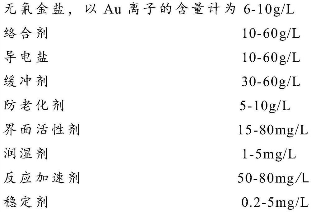
[0060] A kind of cyanide-free chemical gold-plating solution, every 1 liter of described cyanide-free chemical gold-plating solution comprises following composition:
[0061]
[0062] Adjust the pH to 7.2 with sulfuric acid or potassium hydroxide;
[0063] The balance is water.
[0064] Operating temperature: 50°C.
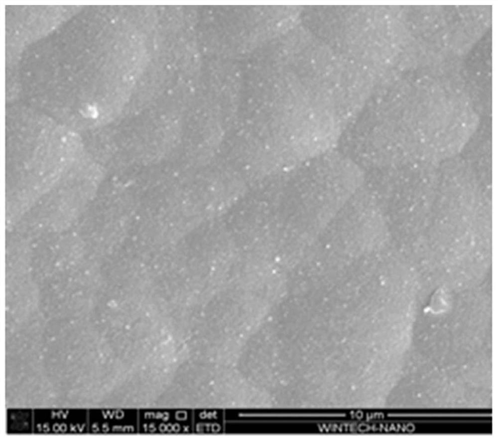
[0065] Using the gold-plating solution prepared by this component, after using the gold-plating method to carry out cyanide-free gold-plating on wafer packaging products, the thickness of the gold finally obtained is 0.3 microns; using the solution and gold-plating process of the present invention, the whole process only needs 20 minutes to complete ; And the crystal size of the obtained gold-plated layer is consistent, without voids and cracks; the surface is smooth.
Embodiment 2
[0067] A kind of cyanide-free chemical gold immersion solution, every 1 liter of described cyanide-free chemical gold immersion solution comprises following composition:
[0068]
[0069] Adjust the pH to 8 with sulfuric acid or potassium hydroxide;
[0070] The balance is water.
[0071] Operating temperature: 60°C.
[0072] Using the gold plating solution prepared by this component, after using the gold plating method to carry out cyanide-free gold plating on wafer packaging products, the gold thickness is 0.2 microns; using the solution and gold plating process of the present invention, the whole process only needs 12 minutes to complete; and obtained The crystallization of the gold-plated layer is consistent in size, without voids or cracks; the surface is smooth.
Embodiment 3
[0074]
[0075]
[0076] Adjust the pH to 9 with sulfuric acid or potassium hydroxide;
[0077] The balance is water.
[0078] Operating temperature: 80°C.
[0079] Using the gold plating solution prepared by this component, after using the gold plating method to carry out cyanide-free gold plating on wafer packaging products, the gold thickness is 0.05 microns; using the solution and gold plating process of the present invention, the whole process only needs 2 minutes to complete; and obtained The crystallization of the gold-plated layer is consistent in size, without voids or cracks; the surface is smooth.
PUM
 Abstract
Description
Claims
Application Information


