GaN single crystal manufacturing device

A technology for manufacturing devices and single crystals, applied in the directions of single crystal growth, single crystal growth, crystal growth, etc., can solve the problem that the large diameter of GaN substrate cannot be widely used, and achieves increased intuitiveness, improved reaction efficiency, and increased reaction Effect of contact area

Active Publication Date: 2021-06-25
WUXI WUYUE SEMICON CO LTD
View PDF6 Cites 0 Cited by
  • Summary
  • Abstract
  • Description
  • Claims
  • Application Information

AI Technical Summary

Problems solved by technology

[0006] Aiming at the deficiencies of the prior art, the present invention provides a GaN single crystal manufacturing device, which solves the problem that the quality improvement and large diameter of the GaN substrate cannot be widely implemented and used

Method used


Image

  • GaN single crystal manufacturing device
  • GaN single crystal manufacturing device

Examples


Embodiment Construction

[0026] The following will clearly and completely describe the technical solutions in the embodiments of the present invention with reference to the accompanying drawings in the embodiments of the present invention. Obviously, the described embodiments are only some, not all, embodiments of the present invention. Based on the embodiments of the present invention, all other embodiments obtained by persons of ordinary skill in the art without making creative efforts belong to the protection scope of the present invention.

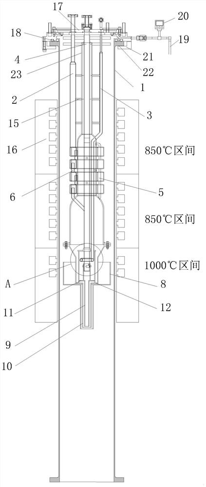
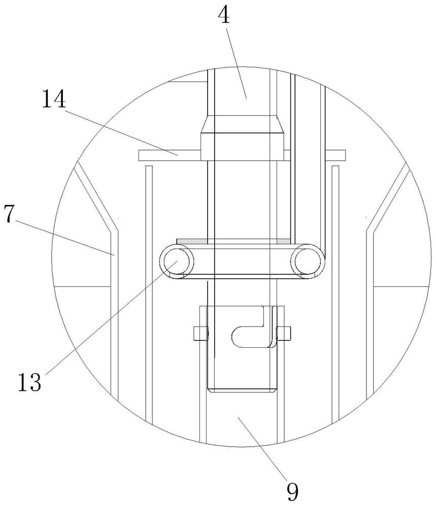
[0027] Such as Figure 1-2 As shown, the present invention provides a technical solution: a GaN single crystal manufacturing device, including a reaction tube 1 made of quartz, a connecting flange 17 and a separation flange 21, and the outer ring of the reaction tube 1 made of quartz is provided with a ring suitable for it. The high-temperature electric furnace 16 of matching, quartz reaction tube 1 is provided with quartz-made introduction tube 2, quartz-made...


PUM


Abstract

The invention relates to the technical field of GaN single crystal preparation, and discloses a GaN single crystal manufacturing device which comprises a quartz reaction pipe, a connecting flange and a separating flange. A high-temperature electric furnace matched with the quartz reaction pipe is annularly arranged on the outer side of the quartz reaction pipe. A quartz guide inlet pipe, a quartz guide gas pipe, a quartz inner container, a quartz outer container, a quartz Ga groove, a quartz spiral reaction pipe, a quartz flange connecting pipe, a quartz stepped outer frame, an inner spray pipe and a middle spray pipe are arranged in the quartz reaction pipe; and a flange plate of the quartz inner container is clamped between two flange plates of the connecting flange. According to the manufacturing device of the GaN single crystal, an HVPE method and an MOCVD method are used in the same device to control the growth of the GaN single crystal, so that the situation that a gallium nitride crystal is cracked when the gallium nitride crystal grows thick or is cooled due to stress caused by a lattice constant and a thermal expansion number can be effectively avoided, and the grown gallium nitride is easy to strip from sapphire when being cooled. The manufacturing and production cost of the product is effectively reduced.

Description

technical field [0001] The invention relates to the related technical field of GaN single crystal preparation, in particular to a GaN single crystal manufacturing device. Background technique [0002] GaN is a typical representative of the third-generation wide-bandgap semiconductors. It has been widely used in semiconductor lighting, microwave power devices, and power electronic devices, showing great application prospects. The most ideal substrate for gallium nitride growth is naturally gallium nitride single crystal material. Such homoepitaxial (that is, the epitaxial layer and the substrate are the same material) can greatly improve the crystal quality of the epitaxial film and reduce the dislocation density. , Improve the working life of the device, improve the luminous efficiency, and increase the working current density of the device. However, gallium nitride single crystal growth is difficult and expensive, and large-scale homoepitaxial growth is still not possible....

Claims


Application Information

Patent Timeline
IPC IPC(8): C30B29/40C30B25/14C30B25/08
CPCC30B25/08C30B25/14C30B29/406
Inventor 山本晓张海涛刘良宏许彬庞博
Owner WUXI WUYUE SEMICON CO LTD
Why Eureka
Try Eureka