

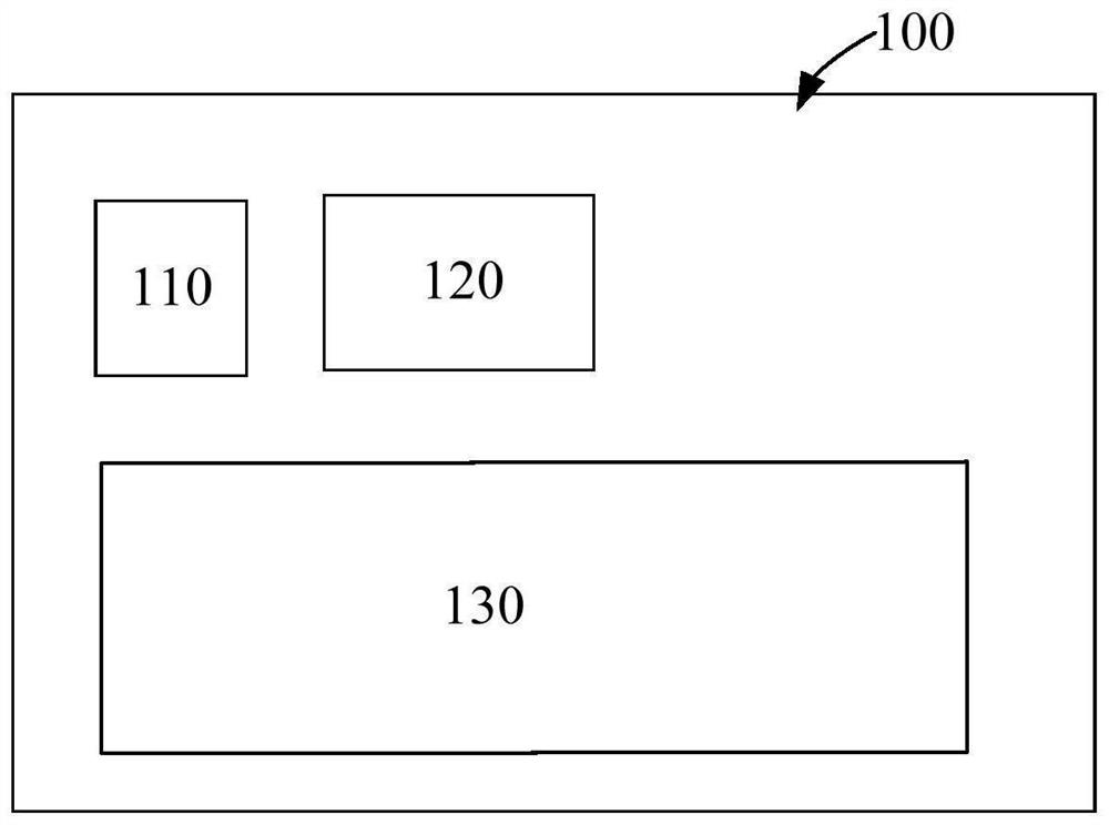
Optical waveguide structure, AR device and manufacturing method of optical waveguide structure
An optical waveguide and columnar structure technology, applied in the field of AR equipment, can solve the problems of complex production process, narrow angle selectivity, affecting production efficiency, etc., and achieve the effect of uniform color, easy processing, and reducing dispersion problems.
- Summary
- Abstract
- Description
- Claims
- Application Information
AI Technical Summary
Problems solved by technology
Method used
Image

Examples
Embodiment Construction
[0033] Embodiments of the present application will be described in more detail below with reference to the accompanying drawings. Although embodiments of the present application are shown in the drawings, it should be understood that the present application may be embodied in various forms and should not be limited by the embodiments set forth herein. Rather, these embodiments are provided so that this application will be thorough and complete, and will fully convey the scope of this application to those skilled in the art.
[0034] The terminology used in this application is for the purpose of describing particular embodiments only, and is not intended to limit the application. As used in this application and the appended claims, the singular forms "a", "the", and "the" are intended to include the plural forms as well, unless the context clearly dictates otherwise. It should also be understood that the term "and / or" as used herein refers to and includes any and all possible ...
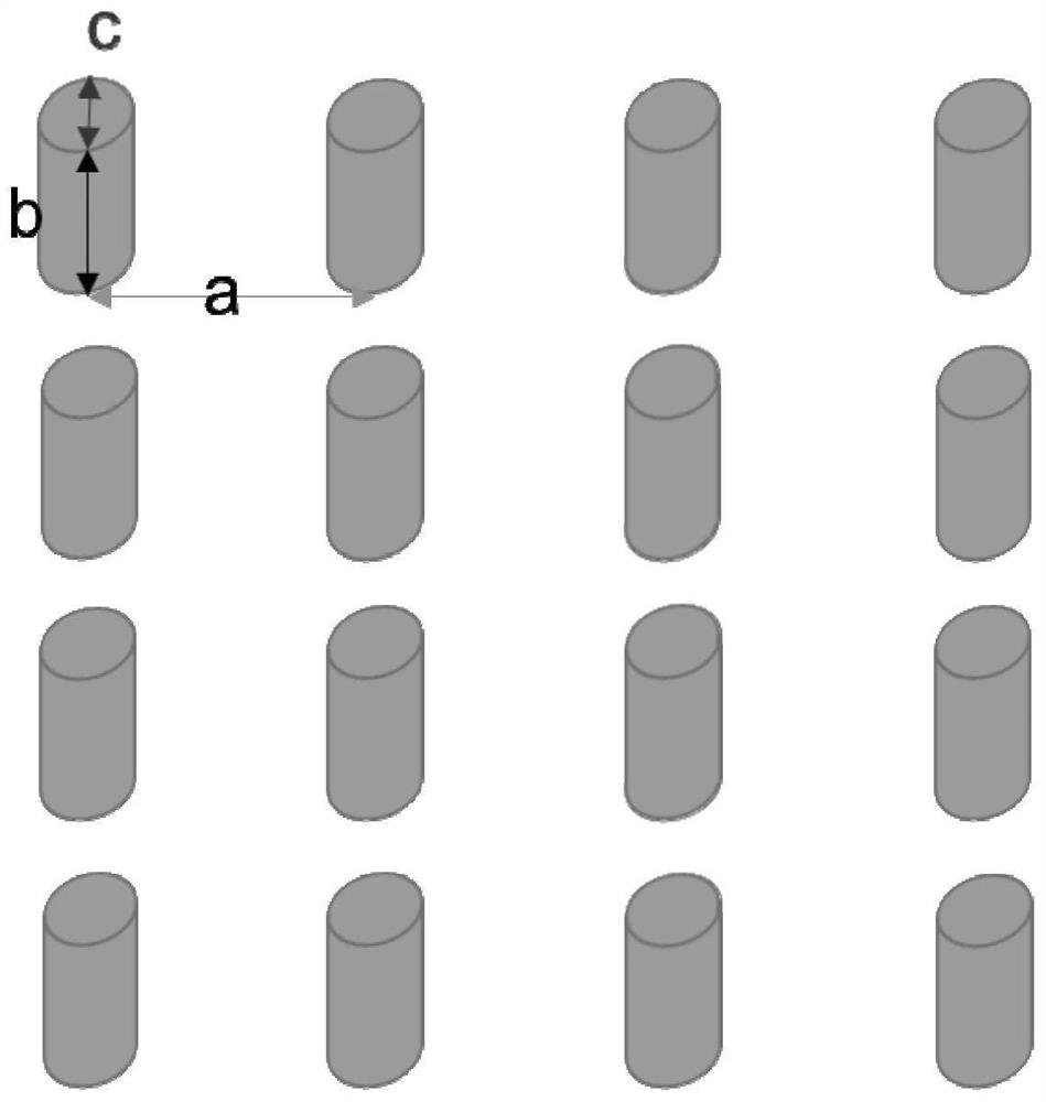
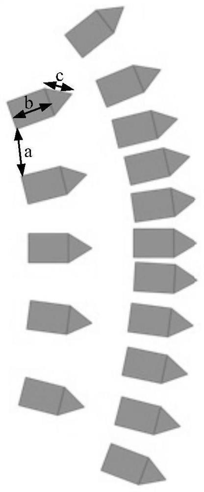
PUM
| Property | Measurement | Unit |
|---|---|---|
| diameter | aaaaa | aaaaa |
| height | aaaaa | aaaaa |
| length | aaaaa | aaaaa |
Abstract
Description
Claims
Application Information