Etching method
A technology to be etched and etched, used in electrical components, semiconductor/solid-state device manufacturing, circuits, etc., and can solve problems affecting the electrical properties and yield of semiconductor devices, poor ion implantation effect, and insufficient photoresist layer mask. and other problems, to ensure the electrical performance, improve the selection ratio, and achieve good mask effect.
- Summary
- Abstract
- Description
- Claims
- Application Information
AI Technical Summary
Problems solved by technology
Method used
Image

Examples
Embodiment Construction
[0028] The following will clearly and completely describe the embodiments of the present application with reference to the accompanying drawings in the embodiments of the present application. Obviously, the described embodiments are only some of the embodiments of the present application, not all of them. Based on the embodiments in this application, all other embodiments obtained by persons of ordinary skill in the art without making creative efforts belong to the scope of protection of this application.
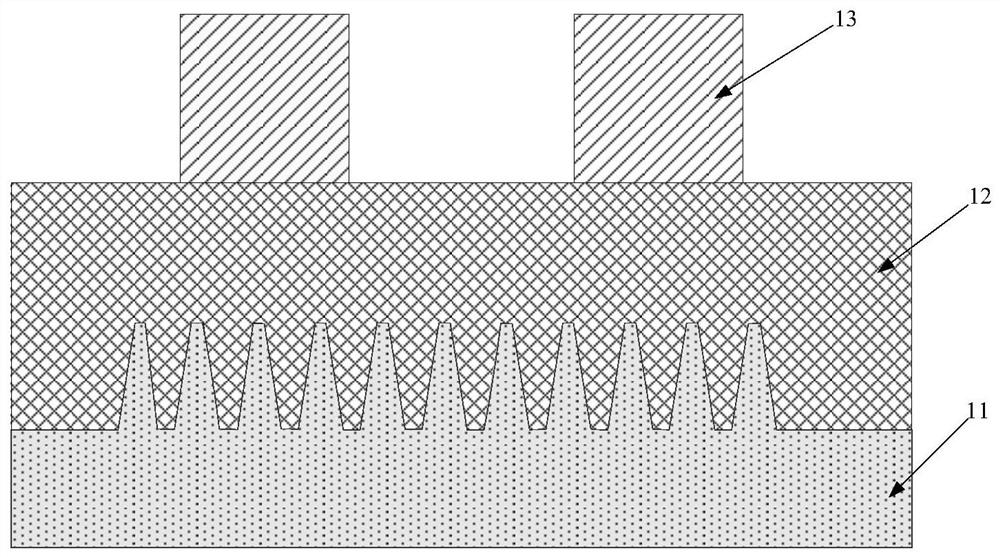
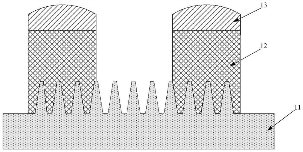
[0029] As described in the background art, in the existing etching process, the selection ratio of the bottom anti-reflection coating to the photoresist layer is between 1:1 and 2:1. In this way, the effective mask of the photoresist layer after etching is not enough, the effect of ion implantation becomes poor, and the implanted area of the PN junction is enlarged, thus affecting the electrical properties and yield of the semiconductor device. Therefore, it is becoming m...
PUM
 Abstract
Description
Claims
Application Information
 - R&D
- Intellectual Property
- Life Sciences
- Materials
- Tech Scout
- Unparalleled Data Quality
- Higher Quality Content
- 60% Fewer Hallucinations
Browse by: Latest US Patents, China's latest patents, Technical Efficacy Thesaurus, Application Domain, Technology Topic, Popular Technical Reports.
© 2025 PatSnap. All rights reserved.Legal|Privacy policy|Modern Slavery Act Transparency Statement|Sitemap|About US| Contact US: help@patsnap.com