Hybrid bonding method and substrate for bonding

A hybrid bonding and bonding technology, which is applied in the fields of semiconductor/solid-state device parts, semiconductor devices, electrical components, etc., can solve the problems of difficult sag control and high process requirements, and achieve the effect of reducing process difficulty and high fault tolerance.

Active Publication Date: 2021-06-25
UNITED MICROELECTRONICS CENT CO LTD
View PDF11 Cites 0 Cited by
  • Summary
  • Abstract
  • Description
  • Claims
  • Application Information

AI Technical Summary

Problems solved by technology

However, this method has high requirements on the process of Cu chemical mechanical polishing, and it is difficult to control the depression, especially for Cu pads of different sizes.

Method used


Image

  • Hybrid bonding method and substrate for bonding
  • Hybrid bonding method and substrate for bonding
  • Hybrid bonding method and substrate for bonding

Examples


Embodiment Construction

[0015] The specific implementation of a hybrid bonding manufacturing method provided by the present invention will be described in detail below in conjunction with the accompanying drawings.

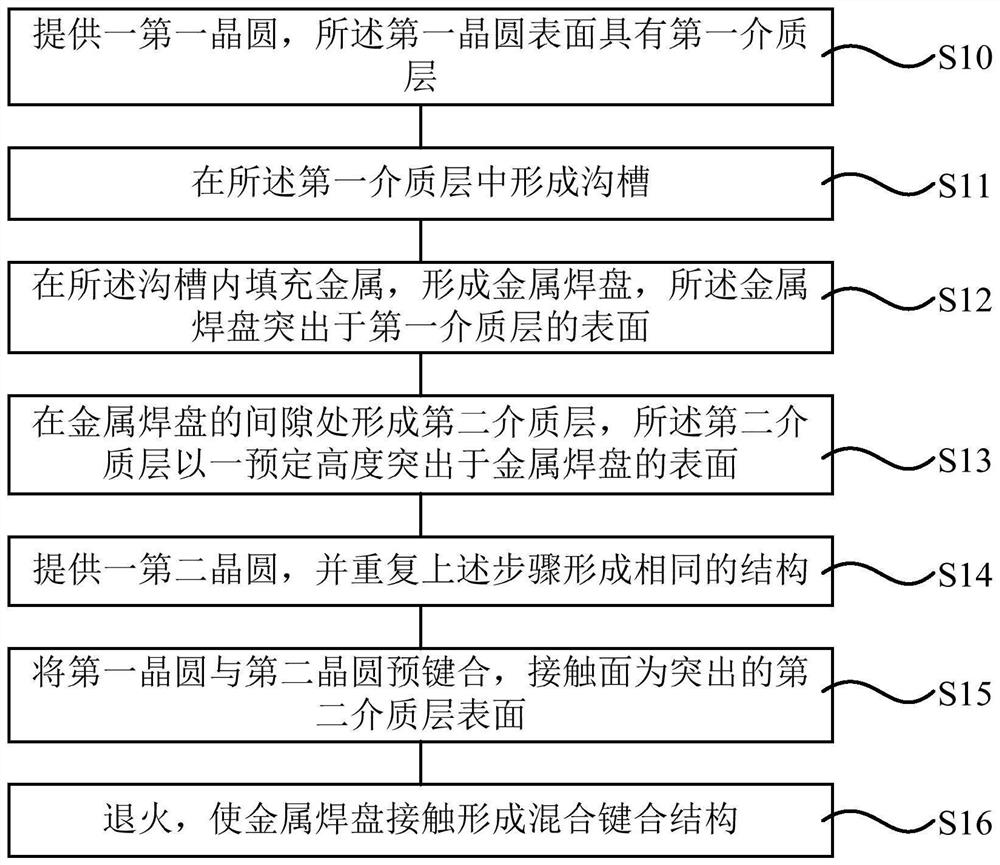
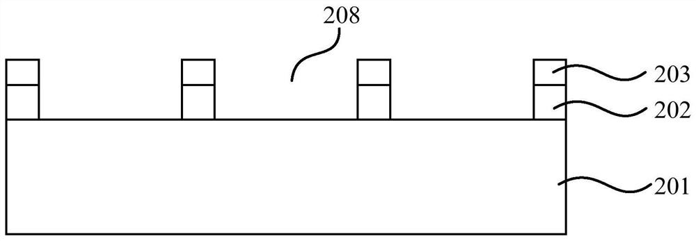
[0016] attached figure 1 Shown is a schematic diagram of the steps of a specific embodiment of the present invention, including: step S10, providing a first wafer, the surface of the first wafer has a first dielectric layer; step S11, in the first dielectric layer Forming a groove; step S12, filling the groove with metal to form a metal pad protruding from the surface of the first dielectric layer; step S13, forming a second dielectric layer at the gap between the metal pads , the second dielectric layer protrudes from the surface of the metal pad with a predetermined height; step S14, providing a second wafer, and repeating the above steps to form the same structure; step S15, combining the first wafer with the second wafer Round pre-bonding, the contact surface is the protruding surfa...


PUM


Abstract

The invention provides a hybrid bonding method and a substrate for bonding. The method comprises the steps of providing a first wafer, wherein the surface of the first wafer is provided with a first dielectric layer; forming a groove in the first dielectric layer; filling the groove with metal to form a metal bonding pad, wherein the metal bonding pad protrudes out of the surface of the first dielectric layer; forming a second dielectric layer at the gap of the metal bonding pad, wherein the second dielectric layer protrudes out of the surface of the metal bonding pad at a preset height; providing a second wafer, and repeating the steps to form the same structure; pre-bonding the first wafer and the second wafer, wherein the contact surface is a protruding second dielectric layer surface; and annealing to enable the metal pads to be in contact to form a hybrid bonding structure. The sinking depth of the metal bonding pad is controlled by accurately controlling the deposition thickness of the dielectric layer, the process is simple, and the error-tolerant rate is high.

Description

technical field [0001] The invention relates to the field of semiconductors, in particular to a hybrid bonding method and a substrate for bonding. Background technique [0002] At present, silicon-based integrated circuits have gradually shown an inflection point, and the industry has entered a mature post-Moore era. Advanced three-dimensional integration technology will have a subversive impact on the innovation of integrated circuits and the industrial structure. Three-dimensional integration technology can vertically bond and stack multi-layer functional units in the Z-axis direction to form an integrated integrated chip system, which solves the problems of multi-dimensional, multi-level and multi-element integration in monolithic technology. It is the development of Moore's Law. The inevitable product of difficulties is the technical basis for realizing system-level 3DSOC. [0003] Bonding technology is an important basis for 3D integration technology. Bonding technolo...

Claims


Application Information

Patent Timeline
Patent Type & Authority Applications(China)
IPC IPC(8): H01L21/60H01L23/498
CPCH01L24/81H01L23/49811H01L23/49838H01L2224/81908
Inventor 李仁雄陈世杰吴罚
Owner UNITED MICROELECTRONICS CENT CO LTD
Why Eureka
Try Eureka