Method for making nanometer dimension triangle air pocket

A technology of nanometer size and manufacturing method, applied in nanostructure manufacturing, nanotechnology, nanotechnology, etc.

Inactive Publication Date: 2010-07-28
INST OF SEMICONDUCTORS - CHINESE ACAD OF SCI
View PDF3 Cites 0 Cited by
  • Summary
  • Abstract
  • Description
  • Claims
  • Application Information

AI Technical Summary

Problems solved by technology

However, there is no public report or record about the fabrication of nanometer-sized triangular air slots

Method used


Image

  • Method for making nanometer dimension triangle air pocket
  • Method for making nanometer dimension triangle air pocket
  • Method for making nanometer dimension triangle air pocket

Examples


Embodiment Construction

[0042] In order to make the object, technical solution and advantages of the present invention clearer, the present invention will be described in further detail below in conjunction with specific embodiments and with reference to the accompanying drawings.

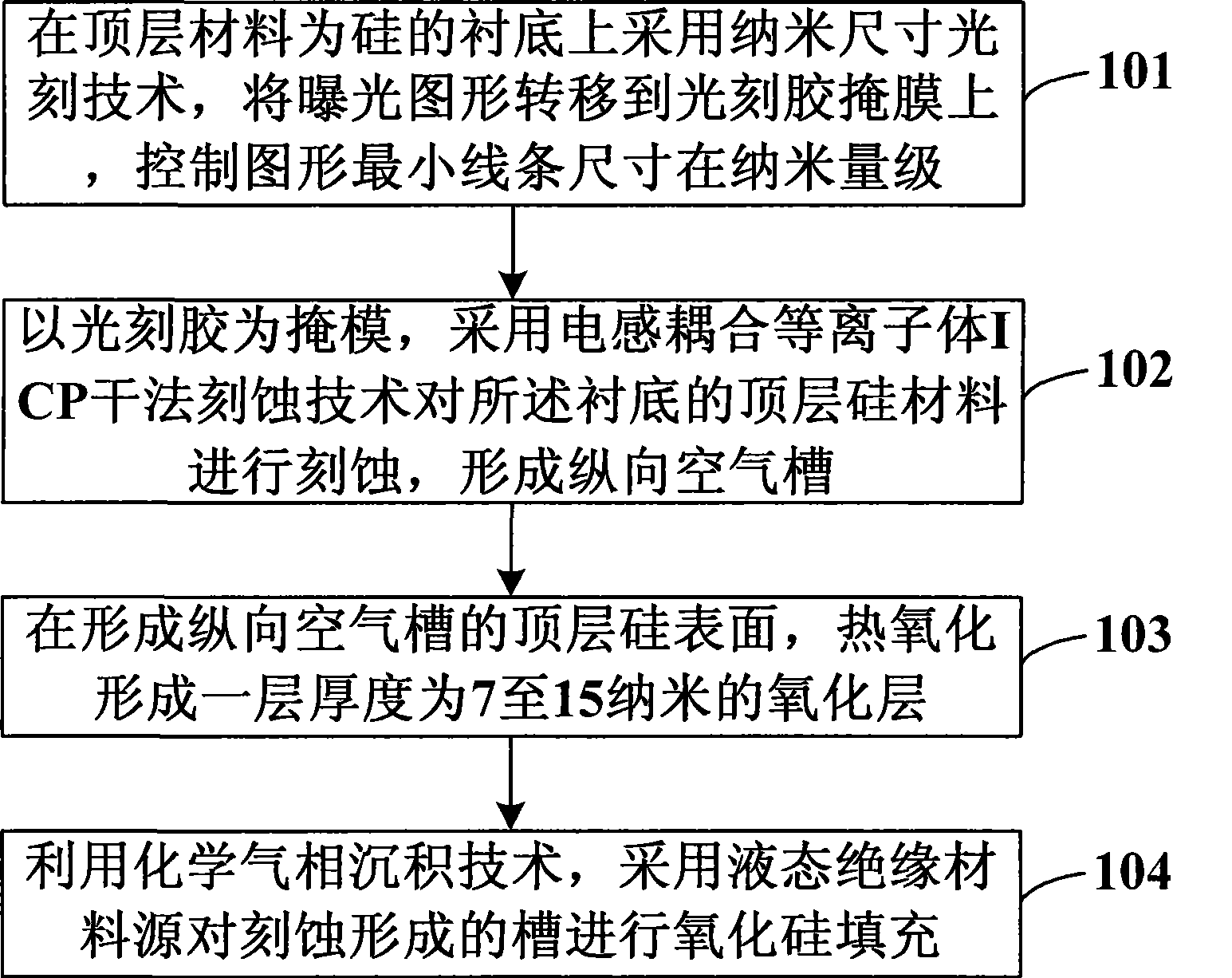
[0043] Such as figure 1 as shown, figure 1 The flow chart of the method for making nano-sized triangular air slots provided by the present invention, the method comprises the following steps:

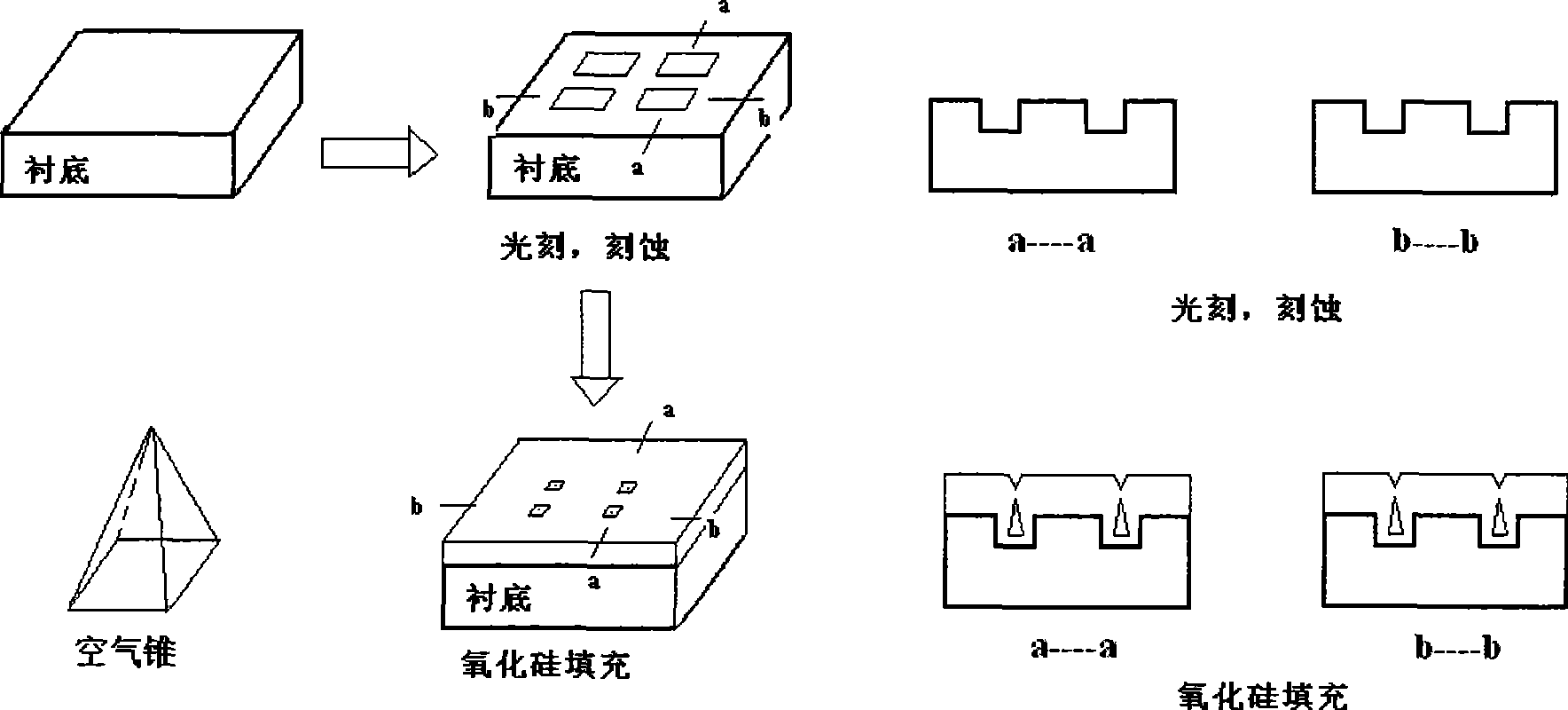
[0044] Step 101: Using nanoscale photolithography technology on the substrate whose top layer material is silicon, transfer the exposure pattern to the photoresist mask, and control the minimum line size of the pattern to be on the order of nanometers;

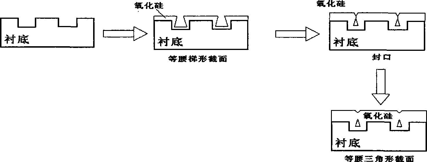
[0045] Step 102: using the photoresist as a mask, using inductively coupled plasma ICP dry etching technology to etch the silicon material on the top layer of the substrate to form vertical air grooves;

[0046] Step 103: forming an oxide layer with a thickness of 7 to 15 nanometer...


PUM


Abstract

The invention discloses a manufacturing method of a nanometer triangular air slot, belonging to the technology field of micro / nano processing techniques. The method comprises the steps of: (1) on a substrate with a silicon top layer, transferring an exposure pattern on a photoresist mask by using nanometer photoetching technique and controlling the minimal line of the pattern at a nanometer scale; (2) etching the top layer silicon of the substrate with the photoresist as a mask by using inductively coupled plasma (ICP) dry etching technique to form a longitudinal air slot; (3) forming an oxidizing layer of thickness 7-15 nanometers on the surface of the top layer silicon forming the longitudinal air slot by thermal oxidization; and (4) filling the etched slot with silicon oxide adopting aliquid state insulating material by using chemical vapor deposition technique. The inventive method can manufacture the nanometer triangular air slot.

Description

technical field [0001] The invention relates to the technical field of micro-nano processing, in particular to a method for manufacturing a nano-sized triangular air groove. Background technique [0002] Microelectronics technology continues to develop in the direction of miniaturization and multi-functional integration, and various advanced micro-nano processing technologies continue to emerge. Among them, the development level of micro-nano-scale exposure technology and etching technology plays a decisive role in the improvement and improvement of device performance. [0003] In recent years, the country has invested a lot of funds in scientific research, various high-quality micro-nano processing equipment has entered major scientific research institutes, and the domestic micro-nano processing technology level has developed rapidly. The high-level micro-nano processing production line provides a huge impetus for the development of microelectronics technology, micro-optic...

Claims


Application Information

Patent Timeline
Patent Type & Authority Patents(China)
IPC IPC(8): H01L21/762B82B3/00
Inventor 屠晓光陈少武
Owner INST OF SEMICONDUCTORS - CHINESE ACAD OF SCI
Why Eureka
Try Eureka