Preparation method of CuI nanostructure

A technology of nanostructure and electron beam evaporation, applied in ion implantation plating, metal material coating process, coating, etc., can solve the problems of low preparation temperature, complicated operation, high preparation temperature, etc., and achieve simple preparation method and large area Uniformity and low reaction temperature

Inactive Publication Date: 2017-08-22
LUDONG UNIVERSITY
View PDF3 Cites 8 Cited by
  • Summary
  • Abstract
  • Description
  • Claims
  • Application Information

AI Technical Summary

Problems solved by technology

However, these preparation technologies have disadvantages such as high vacuum conditions, complicated equipment operation, and high preparation temperature.
In addition, people have also studied chemical preparation methods such as (electro)chemical synthesis, high-temperature iodination, and sol-gel to prepare CuI thin films or nanostructures. Although these technologies have simple equipment, they have disadvantages such as long reaction time and complicated operation.
B.A.Nejand et al. used a hydrothermal evaporation method to prepare CuI nanostructures (MaterialsLetters 132 (2014) 138-140). This method has low preparation temperature, short reaction time and high material crystallization quality, but there are problems with material growth. The disadvantage of uniformity cannot meet the needs of large-area device applications

Method used


Image

  • Preparation method of CuI nanostructure
  • Preparation method of CuI nanostructure
  • Preparation method of CuI nanostructure

Examples


Embodiment 1

[0025] A method for preparing a CuI nanostructure, comprising the steps of:

[0026] 1) The monocrystalline silicon (100) substrate is cleaned by standard RCA to remove organic matter, metal ion impurities and dust on the surface, blown dry with nitrogen gas, and put it into the vacuum growth chamber of the electron beam evaporation device;

[0027] 2) Electron beam evaporation method grows a layer of copper thin film on the surface of single crystal silicon (100) substrate, and its specific process condition is that the background vacuum is 5×10 -4 ~3×10 -3 pa, the substrate temperature is 25-30°C, the growth rate is 0.15nm / s, the purity of the copper evaporation source used is 99.999wt%, and the thickness of the obtained copper film is 200nm;

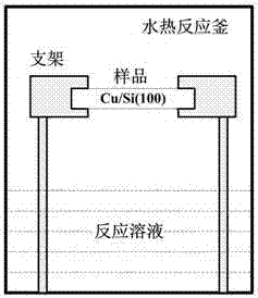
[0028] 3) with step 2) gained silicon-based copper thin film such as figure 1 The suspension shown in the reactor, CuCl in the precursor solution of the reactor 2 The concentration of polyvinylpyrrolidone is 0.1mol / L, the concentra...

Embodiment 2

[0032] A method for preparing a CuI nanostructure, comprising the steps of:

[0033] 1) The monocrystalline silicon (100) substrate is cleaned by standard RCA to remove organic matter, metal ion impurities and dust on the surface, blown dry with nitrogen gas, and put it into the vacuum growth chamber of the electron beam evaporation device;

[0034] 2) Electron beam evaporation method grows a layer of copper thin film on the surface of single crystal silicon (100) substrate, and its specific process condition is that the background vacuum is 5×10 -4 ~3×10 -3 pa, the substrate temperature is 25-30°C, the growth rate is 0.15nm / s, the purity of the copper evaporation source used is 99.999wt%, and the thickness of the obtained copper film is 50nm;

[0035] 3) with step 2) gained silicon-based copper thin film such as figure 1 The suspension shown in the reactor, CuCl in the precursor solution of the reactor 2 The concentration of polyvinylpyrrolidone is 0.05mol / L, the concentra...

Embodiment 3

[0039] A method for preparing a CuI nanostructure, comprising the steps of:

[0040] 1) The monocrystalline silicon (100) substrate is cleaned by standard RCA to remove organic matter, metal ion impurities and dust on the surface, blown dry with nitrogen gas, and put it into the vacuum growth chamber of the electron beam evaporation device;

[0041] 2) Electron beam evaporation method grows a layer of copper thin film on the surface of single crystal silicon (100) substrate, and its specific process condition is that the background vacuum is 5×10 -4 ~3×10 -3 pa, the substrate temperature is 25-30°C, the growth rate is 0.15nm / s, the purity of the copper evaporation source used is 99.999wt%, and the thickness of the obtained copper film is 50nm;

[0042] 3) with step 2) gained silicon-based copper thin film such as figure 1 The suspension shown in the reactor, CuCl in the precursor solution of the reactor 2 The concentration of polyvinylpyrrolidone is 2mol / L, the concentratio...


PUM


Abstract

The invention relates to a method for preparing a CuI nanostructure, comprising the following steps: cleaning the surface of a single crystal silicon substrate, and putting it into a vacuum growth chamber of an electron beam evaporation device; growing on the surface of a single crystal silicon by electron beam evaporation A layer of copper film; the obtained silicon-based copper film is suspended in the reactor, placed horizontally above the solution, and the precursor solution in the reactor is CuCl 2 , a mixed aqueous solution of polyvinylpyrrolidone and KI; seal the reactor and place it in a blast drying oven for hydrothermal reaction at 120-200°C; after the reaction, take out the sample, wash it, and dry it. For the first time, the present invention uses Cu film and iodine vapor evaporated by hydrothermal synthesis as reaction raw materials to prepare large-area and uniform CuI nanomaterials under low temperature and high pressure conditions, and the preparation process is compatible with the preparation process of optoelectronic devices.

Description

technical field [0001] The invention relates to a preparation method of a CuI nanostructure, which belongs to the technical field of semiconductor materials. Background technique [0002] CuI is a wide-bandgap semiconductor material with direct bandgap, the bandgap width is 3.1eV, and the exciton binding energy is as high as about 62meV. The CuI material has a high transmittance (80%) in the visible light region. Because CuI materials generally have excess iodide ions and cause copper vacancy defects, they exhibit p-type conductivity and high hole mobility (>40cm 2 V -1 the s -1 ). In addition, CuI has the advantages of non-toxicity, abundant reserves, and low cost. These advantages make CuI materials show broad application prospects in the fields of solar cells, photodetectors, photoelectric sensors, display devices and transparent conductive films. [0003] At present, people have realized the preparation of CuI thin films and nanostructures by various methods, in...

Claims


Application Information

Patent Timeline
Patent Type & Authority Applications(China)
IPC IPC(8): C23C14/30C23C14/16C23C14/58
CPCC23C14/30C23C14/16C23C14/5846
Inventor 张立春杨立新林国琛赵风周曲崇
Owner LUDONG UNIVERSITY
Why Eureka
Try Eureka