Method for producing organic electroluminescence device

An electroluminescent device and device technology, which is applied in the fields of electro-solid devices, semiconductor/solid-state device manufacturing, electrical components, etc., to achieve the effects of compatible preparation processes, easy operation, and increased injection efficiency

Inactive Publication Date: 2009-09-23
UNIV OF ELECTRONICS SCI & TECH OF CHINA
View PDF0 Cites 10 Cited by
  • Summary
  • Abstract
  • Description
  • Claims
  • Application Information

AI Technical Summary

Problems solved by technology

However, there are few reports on the preparation of composite nanomaterials for PEDOT nanoparticles. Due to the difficulty in obtaining a well-dispersed polymer system, PEDOT nanoparticles cannot fully exert their high electrical conductivity. Therefore, an effective method is used to obtain super Thin, uniformly dispersed PEDOT nanoparticle composite films are of great significance for preparing high-performance hole injection layers and improving the performance of organic electroluminescent devices

Method used


Image

  • Method for producing organic electroluminescence device

Examples


Embodiment 1

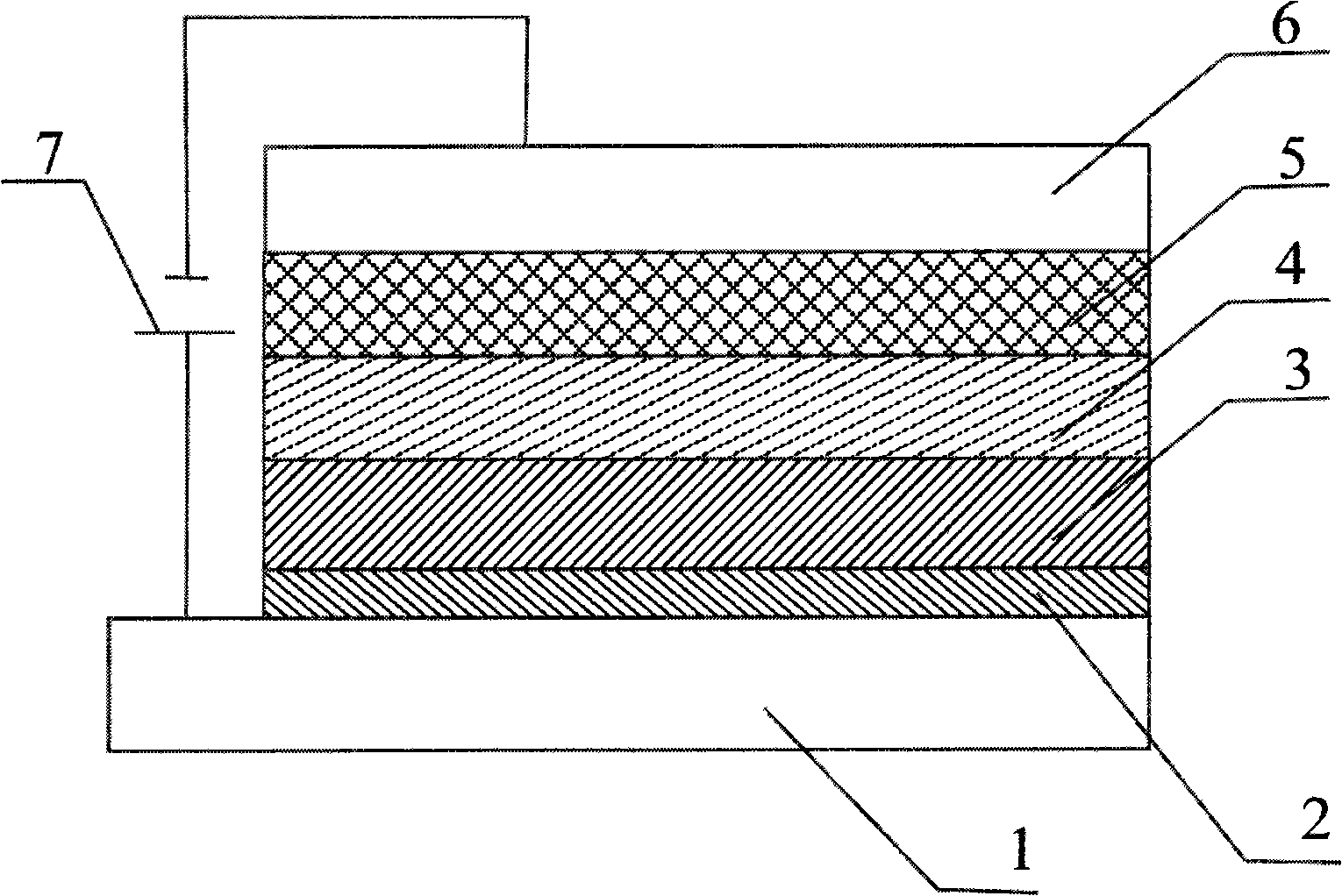
[0062] Such as figure 1 As shown, the organic functional layers in the device structure include a hole transport layer 3, a light emitting layer 4 and an electron transport layer 5, wherein the light emitting layer 4 is a blue light emitting layer or a green light emitting layer respectively.

[0063] The material of the hole transport layer of the device is NPB, and the material of the light emitting layer is BAlq or Alq 3 , the electron transport material is Alq 3 , The cathode layer is made of Mg:Ag alloy. The entire device structure is described as:

[0064] Glass substrate / ITO / {3,4-polyethylenedioxythiophene / polystyrenesulfonic acid / 3,4-polyethylenedioxythiophene nanoparticles (particle size 20nm) / NPB (30nm) / BAlq (10nm ) / Alq 3 (10nm) / Mg:Ag(90nm)

[0065] The preparation method is as follows:

[0066] (1) Utilize detergent, ethanol solution and deionized water to ultrasonically clean the anode substrate, and dry it with dry nitrogen after cleaning;

[0067] (2) Ultr...

Embodiment 2

[0074] Such as figure 1 As shown, the organic functional layers in the device structure include a hole transport layer 3, a light emitting layer 4 and an electron transport layer 5, wherein the light emitting layer 4 is a blue light emitting layer or a green light emitting layer respectively.

[0075] The material of the hole transport layer of the device is NPB, and the material of the light emitting layer is BAlq or Alq 3 , the electron transport material is Alq 3 , The cathode layer is made of Mg:Ag alloy. The entire device structure is described as:

[0076] Glass substrate / ITO / {3,4-polyethylenedioxythiophene / polystyrenesulfonic acid / 3,4-polyethylenedioxythiophene nanoparticles (particle size 30nm) / NPB (30nm) / BAlq (10nm ) / Alq 3 (10nm) / Mg:Ag(90nm)

[0077] The manufacturing process of the device is the same as that of Embodiment 1

Embodiment 3

[0079] Such as figure 1 As shown, the organic functional layers in the device structure include a hole transport layer 3, a light emitting layer 4 and an electron transport layer 5, wherein the light emitting layer 4 is a blue light emitting layer or a green light emitting layer respectively.

[0080] The material of the hole transport layer of the device is NPB, and the material of the light emitting layer is BAlq or Alq 3 , the electron transport material is Alq 3 , The cathode layer is made of Mg:Ag alloy. The entire device structure is described as:

[0081] Glass substrate / ITO / {3,4-polyethylenedioxythiophene / polystyrenesulfonic acid / polypyrrole nanoparticles (particle size 20nm) / NPB(30nm) / BAlq(10nm) / Alq 3 (10nm) / Mg:Ag(90nm)

[0082] The manufacturing process of the device is the same as that of Embodiment 1


PUM


Abstract

The invention discloses a method for producing an organic electroluminescence device. The method comprises the followings steps: frirstly, conducting polymer or conducting polymer nano-particle composite materials are formed on the anode of a device, and are used as the hole injection layers of the device; and secondly, other functional layers and membrane electrodes of the device are produced. The conducting polymers in the hole injection layers include conducting polymers and nano-particles thereof, and the device has the characteristics of high electrical conductivity and good membrane planeness. The method can not only be used for producing the organic electroluminescence device with the advantages of high luminous efficiency and long service life, but also can be applied to the fields of backlights, luminance light panels, and the like for color LED display.

Description

technical field [0001] The invention relates to the technical field of organic electroluminescence in electronic components, in particular to a preparation method of an organic electroluminescence device. Background technique [0002] In recent years, the conductive polymer poly-3,4-ethylenedioxythiophene (PEDOT) has gradually become a hot spot in the research of organic electronic materials due to its high electrical conductivity, thermal stability and good transparency. Doped PEDOT has high electrical conductivity and is a hole-rich material, so it can be used as a hole-transporting material for organic electronic devices. Subsequently, Bayer obtained a water-soluble poly-3,4-ethylenedioxythiophene / polystyrene sulfonic acid (PEDOT:PSS) conductive polymer colloid with adjustable conductivity through the method of copolymerization, which has It has good environmental stability, good electron blocking properties and transparency, and has good affinity for ITO, making it an i...

Claims


Application Information

Patent Timeline
Patent Type & Authority Applications(China)
IPC IPC(8): H01L51/56H01L51/54H01L51/52
Inventor 杨亚杰蒋亚东徐建华
Owner UNIV OF ELECTRONICS SCI & TECH OF CHINA
Why Eureka
Try Eureka