Reverse blocking type IGBT and manufacturing method therefor

A reverse-resistance type and N-type technology, which is applied in semiconductor/solid-state device manufacturing, electrical components, circuits, etc., can solve the problem of reducing device switching speed, poor reverse blocking ability of FS-IGBT structure, and short-circuit safe working area of ​​devices. Bad question

Inactive Publication Date: 2018-03-13
UNIV OF ELECTRONICS SCI & TECH OF CHINA
View PDF8 Cites 8 Cited by
  • Summary
  • Abstract
  • Description
  • Claims
  • Application Information

AI Technical Summary

Problems solved by technology

[0005] The implementation of method (1) will increase the gate-emitter capacitance and gate-collector capacitance at the same time, and the switching process of the IGBT is essentially the process of charging/discharging the gate capacitance, so the increase in the gate capacitance will Makes the charging/discharging time longer, which in turn causes the switching speed to decrease
Therefore, the deep trench gate depth will reduce the switching speed of the device, increase the switching loss of the device, and affect the compromise characteristics of the device's conduction voltage drop and switching loss; and the implementatio

Method used


Image

  • Reverse blocking type IGBT and manufacturing method therefor
  • Reverse blocking type IGBT and manufacturing method therefor
  • Reverse blocking type IGBT and manufacturing method therefor

Examples


Embodiment 1

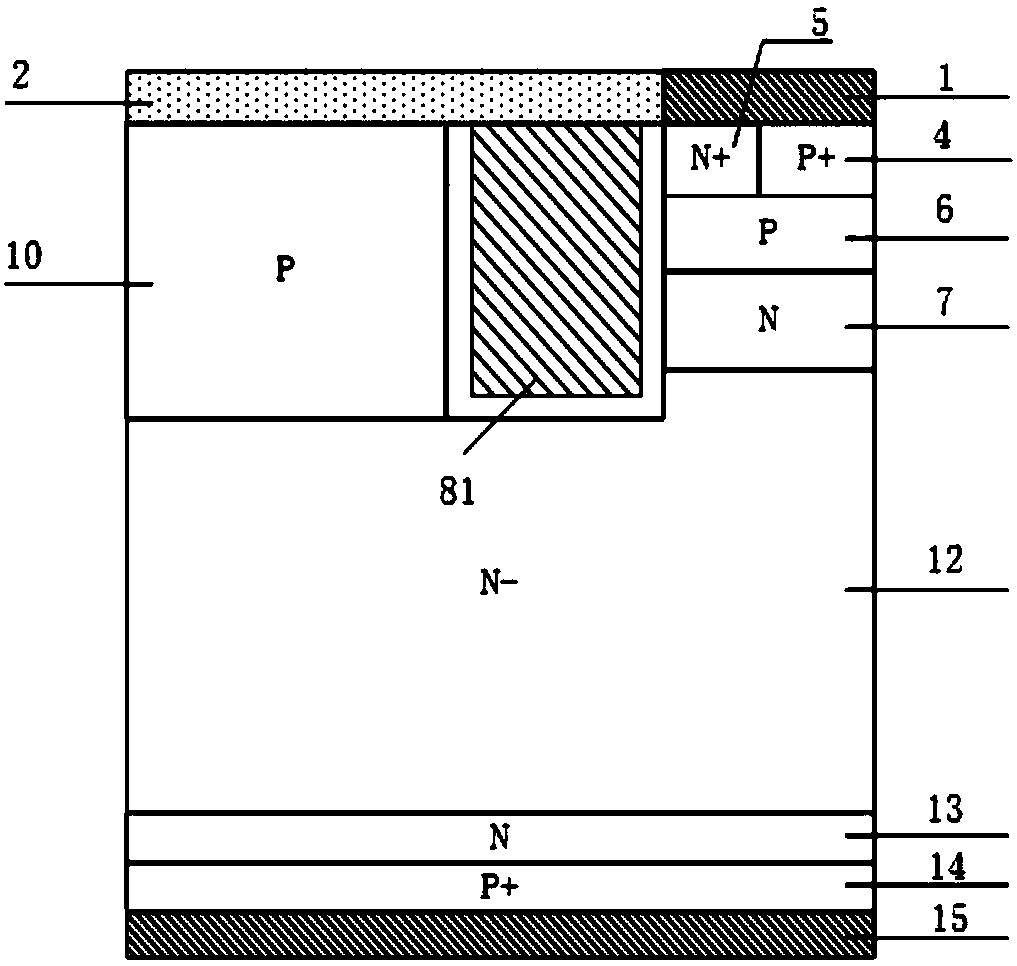
[0102] This embodiment provides a reverse resistance type IGBT, such as figure 2 Its cell structure shown includes: P-type collector region 14, collector metal 15 on the back of P-type collector region 14, N-type electric field stop layer 13 on the front of P-type collector region 14, and N-type electric field stopper layer 13 on the front of P-type collector region 14. The N-type drift region 12 above the layer 13; it is characterized in that: the N-type drift region 12 has a P+ emitter region 4, an N+ emitter region 5, a P-type base region 6, an N-type charge storage layer 7, a P-type body region 10, Trench gate structure, trench emitter structure and trench collector structure;

[0103] The trench emitter structure is located in the center of the top layer of the N-type drift region 12 and penetrates into it along the vertical direction of the device. The emitter dielectric layer 92 is composed of; the N-type drift region 12 on one side of the trench emitter structure has...

Embodiment 2

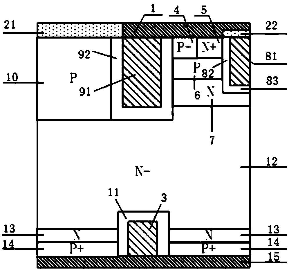
[0105] This embodiment provides a reverse resistance type IGBT, the cell structure of which is as follows image 3 As shown, in this embodiment, except that three identical and independent trench collector structures are arranged in the N-type field stop layer and the P-type collector region on the back of the device, the other structures are the same as in Embodiment 1.

[0106] Compared with Embodiment 1, this embodiment further improves the reverse breakdown voltage of the device.

Embodiment 3

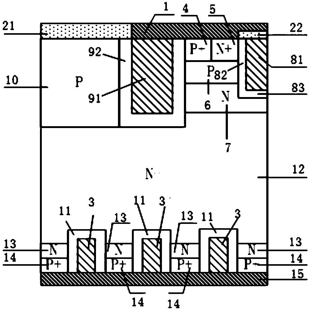
[0108] This embodiment provides a reverse resistance type IGBT, the cell structure of which is as follows Figure 4 As shown, the structure of this embodiment is the same as that of Embodiment 1 except that the first P-type layer 16 connected thereto is disposed under the trench emitter structure.

[0109] In this embodiment, by introducing the first P-type layer 16 connected to the trench emitter electrode 91 through the emitter dielectric layer 92 on the bottom side, the first P-type layer 16 extends laterally to one side to the bottom of the N-type charge storage layer 7 In the N-type drift region 12, the breakdown voltage of the device is improved, and at the same time, the contradiction between the breakdown voltage caused by the concentration of the charge storage layer and the forward conduction voltage drop is improved.


PUM

PropertyMeasurementUnit
Thicknessaaaaaaaaaa
Thicknessaaaaaaaaaa

Abstract

The invention discloses a reverse blocking type IGBT and a manufacturing method therefor, and belongs to the technical field of a semiconductor power device. By introducing trench emitter and trench collector structures, the reverse breakdown voltage of a device is improved without influencing the threshold voltage and switch-on of an IGBT device; the overall gate capacitance is lowered, the switching speed of the device is improved, the switching loss and driving power consumption of the device are lowered, and the compromising relation between forward switch-on voltage drop and switch-off loss of the conventional CSTBT structure is improved; the problems of current, voltage oscillation and EMI in the device starting dynamic process can be avoided, and device reliability is improved; theelectric field concentration effect at the bottom of the trench is improved, the forward breakdown voltage of the device is improved, and reliability of the device is further improved; and the currentcarrier enhancement effect at the emitter end of the device is further improved, the current carrier concentration distribution in a drift region can be improved, and compromising between forward switch-on voltage drop and switch-off loss can be further improved. The manufacturing method disclosed in the invention is compatible with the existing manufacturing process of a CSTBT device.

Description

technical field [0001] The invention belongs to the technical field of semiconductor power devices, in particular to an insulated gate bipolar transistor (IGBT), in particular to a reverse resistance IGBT and a manufacturing method thereof. Background technique [0002] Insulated gate bipolar transistor (IGBT), as one of the core electronic components in modern power electronic circuits, is widely used in various fields such as transportation, communication, household appliances, and aerospace. Insulated gate bipolar transistor (IGBT) is a new type of power electronic device composed of an insulated field effect transistor (MOSFET) and a bipolar junction transistor (BJT), which can be equivalent to a MOSFET driven by a bipolar junction transistor. . IGBT combines the working mechanism of MOSFET structure and bipolar junction transistor. It not only has the advantages of MOSFET easy to drive, low input impedance, and fast switching speed, but also has the advantages of BJT o...

Claims


Application Information

Patent Timeline
IPC IPC(8): H01L29/739H01L21/331H01L29/06
CPCH01L29/0603H01L29/0684H01L29/66325H01L29/7393
Inventor 张金平赵倩刘竞秀李泽宏任敏张波
Owner UNIV OF ELECTRONICS SCI & TECH OF CHINA
Why Eureka
Try Eureka