Preparation method of CsPbI3 thin film

A technology of thin film and single crystal silicon, which is applied in the field of preparation of CsPbI3 thin film, can solve the problems of complex preparation method and low film quality, and achieve the effect of simple preparation method, compatible preparation process and low reaction temperature

Inactive Publication Date: 2018-04-06
LUDONG UNIVERSITY
View PDF4 Cites 9 Cited by
  • Summary
  • Abstract
  • Description
  • Claims
  • Application Information

AI Technical Summary

Problems solved by technology

[0005] The application provides a CsPbI 3 The preparation method of thin film, to solve the CsPbI that prior art prepares 3 The film quality is not high, the preparation method is complicated and other technical problems

Method used


Image

  • Preparation method of CsPbI3 thin film
  • Preparation method of CsPbI3 thin film
  • Preparation method of CsPbI3 thin film

Examples


Embodiment

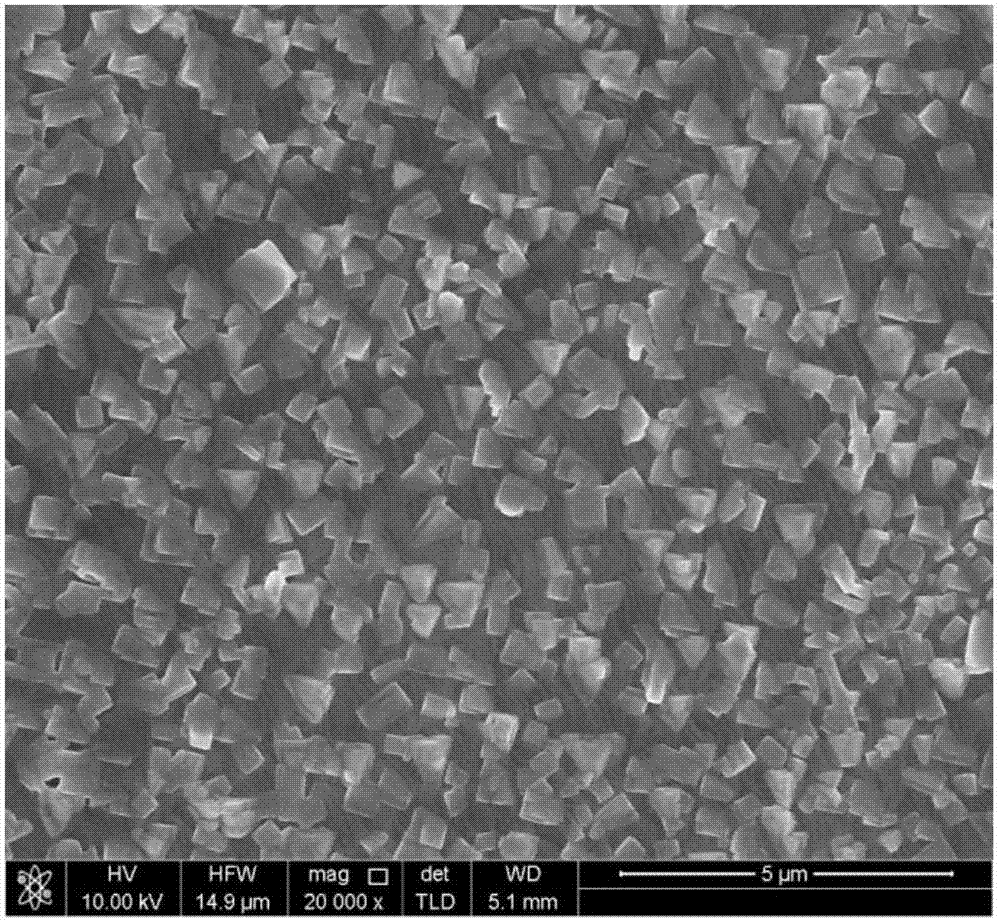
[0033] a CsPbI 3 Thin film preparation method, using laser pulse deposition technology to etch CsPbI 3 Target material, all-inorganic CsPbI prepared under vacuum conditions 3 Perovskite film, that is, the target is placed in the vacuum growth chamber of the pulsed laser deposition system, and the high-power pulsed laser is used to etch CsPbI at high temperature 3 The target material forms a plasma plume, undergoes adiabatic expansion of the plasma, and finally directional diffuses to the silicon substrate to nucleate and grow, forming CsPbI 3 film.

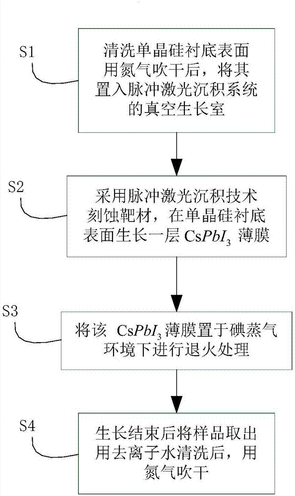
[0034] Such as figure 1 As shown, it specifically includes the following steps:

[0035] S1: Clean the surface of the single crystal silicon substrate, dry it with nitrogen, and put it into the vacuum growth chamber of the pulsed laser deposition system;

[0036] Perform standard RCA cleaning on the monocrystalline silicon substrate to remove organic matter, metal ion impurities and dust on the surface;

[0037] S2: The targ...


PUM

PropertyMeasurementUnit
thicknessaaaaaaaaaa
thicknessaaaaaaaaaa
diameteraaaaaaaaaa

Abstract

The invention provides a preparation method of a CsPbI3 thin film. The preparation method includes the following steps that the surface of a monocrystalline silicon substrate is cleaned, and the monocrystalline silicon substrate is placed in a vacuum growth room of a pulse laser deposition system after the surface is blown to be dry through nitrogen; a target material is etched through the pulse laser deposition technology, and a layer of CsPbI3 thin film grows on the surface of monocrystalline silicon; the CsPbI3 thin film is placed under an iodine steam environment to be subjected to annealing treatment, and in other words, the CsPbI3 thin film is recrystallized under the iodine steam environment; and a sample is taken out after growth ends, is cleaned with deionized water and is blown to be dry through nitrogen. The preparation method is simple, the reaction temperature is low, the reaction time is short, cost is low, and the preparation method is suitable for industrialized production; and the large-area uniform and compact CsPbI3 thin film high in crystallization quality and excellent in photoelectric property can be obtained, and application of the CsPbI3 thin film to the field of photoelectric devices such as luminescent materials and solar cells is met.

Description

technical field [0001] The invention relates to the field of semiconductor materials, in particular to a CsPbI 3 The method of film preparation. Background technique [0002] In recent years, some semiconductor materials with perovskite structure have become a research hotspot in the field of solar cells due to their excellent optical absorption and charge conduction properties. Compared with organic-inorganic hybrid perovskite materials, all-inorganic halogen perovskite materials (CsPbX 3 , X=Cl, Br, I) have high chemical stability, and have extremely high fluorescence quantum efficiency (up to 90%), adjustable fluorescence wavelength and cover the entire visible light band, narrow line width, etc., and are expected to be applied to the new generation of display and lighting technology. In addition, the all-inorganic perovskite material has a very high absorption coefficient, and its light absorption capacity is more than 10 times higher than that of other organic dyes; ...

Claims


Application Information

Patent Timeline
Patent Type & Authority Applications(China)
IPC IPC(8): C23C14/28C23C14/06C23C14/58
CPCC23C14/28C23C14/0694C23C14/5806
Inventor 张立春林国琛薛晓娥赵风周徐满
Owner LUDONG UNIVERSITY
Why Eureka
Try Eureka