Trench mosfet and manufacturing method of the same

A technology of oxide semiconductor and field effect transistor, which is applied in semiconductor/solid-state device manufacturing, semiconductor devices, electrical components, etc., can solve the problems of device damage, device temperature rise, performance deterioration, etc., to inhibit turn-on and reduce body resistance. rate, the effect of improving UIS capabilities

Active Publication Date: 2021-06-25
EXCELLIANCE MOS
View PDF6 Cites 1 Cited by
  • Summary
  • Abstract
  • Description
  • Claims
  • Application Information

AI Technical Summary

Problems solved by technology

Once the body resistance becomes high, it will easily cause the parasitic N (source 104)-P (body 106)-N (epitaxial layer 102) bipolar transistor to be turned on, and the MOSFET will undergo secondary breakdown (Secondary breakdown), causing the temperature of the device to rise , causing permanent damage to the device, that is, the performance of the Unclamped Inductive Switching (UIS) deteriorates

Method used


Image

  • Trench mosfet and manufacturing method of the same
  • Trench mosfet and manufacturing method of the same
  • Trench mosfet and manufacturing method of the same

Examples


Embodiment Construction

[0044] Reference will now be made in detail to the exemplary embodiments of the present invention, examples of which are illustrated in the accompanying drawings. The following disclosure provides many different embodiments, or examples, for implementing different features of the invention. Of course, these embodiments are only examples, and are not intended to limit the scope and application of the present invention. Furthermore, the relative thicknesses and positioning of various features, layers or regions may be reduced or exaggerated for clarity. Wherever possible, the same reference numbers will be used in the drawings and description to refer to the same or like parts.

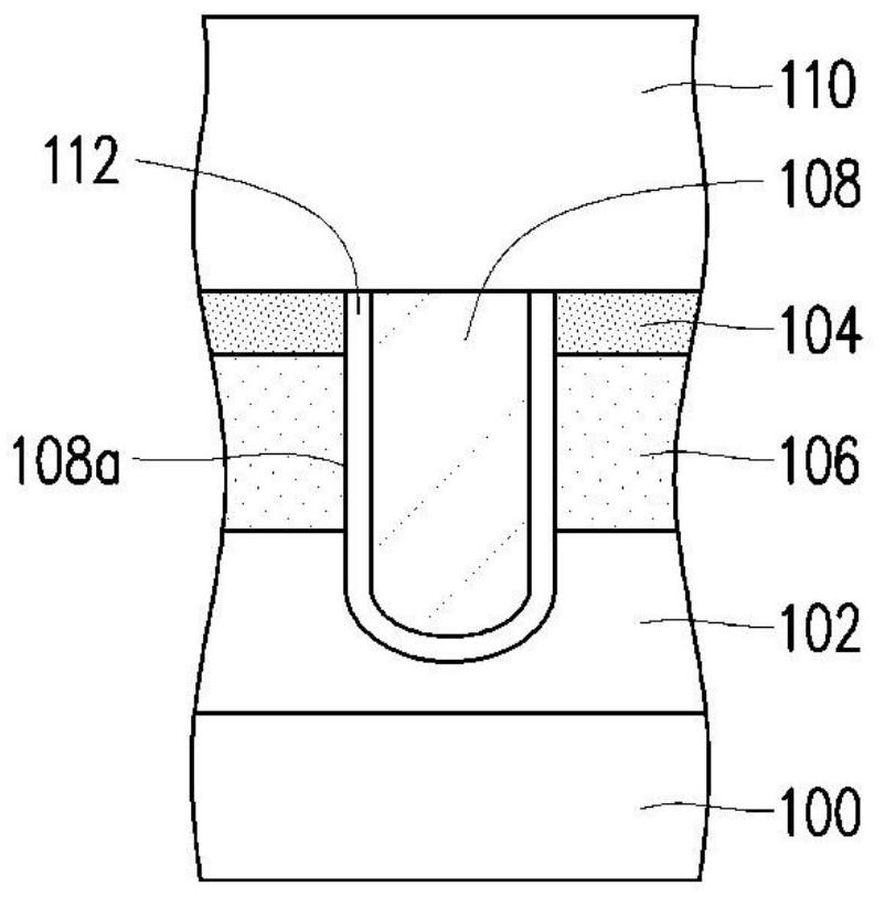
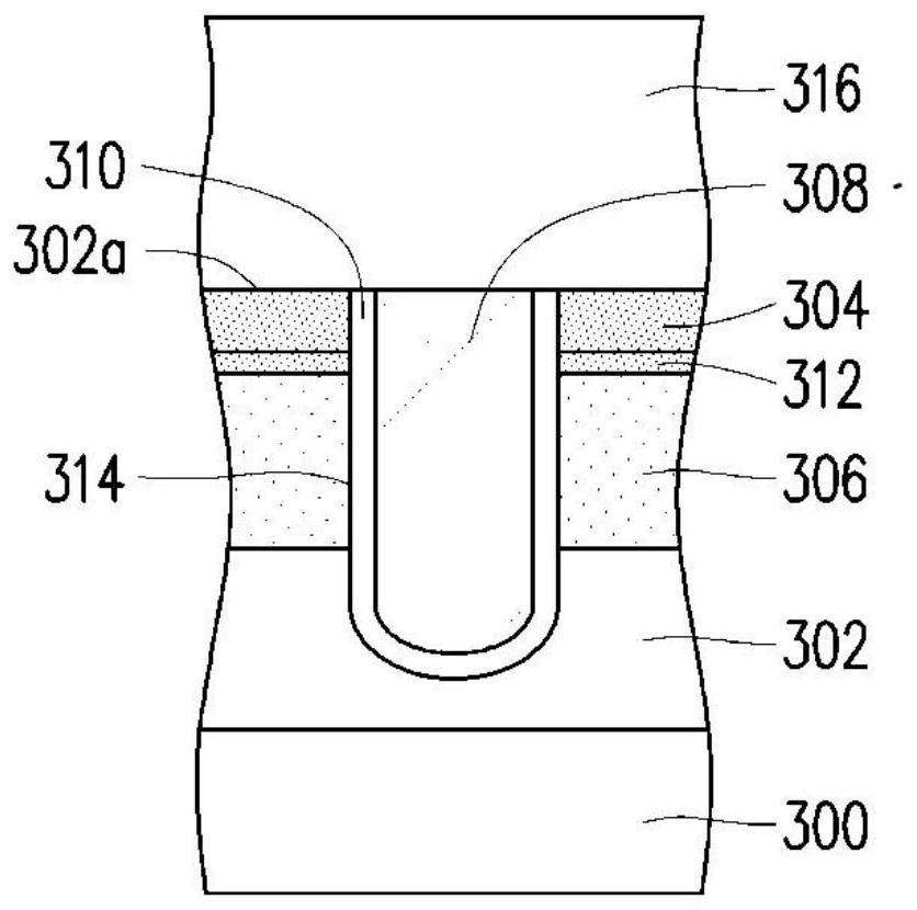
[0045] image 3 is a schematic diagram of a trench MOSFET device according to the first embodiment of the present invention.

[0046] Please refer to image 3 , the trench MOSFET device of the first embodiment includes a substrate 300, an epitaxial layer 302 having a first conductivity type, a sourc...


PUM


Abstract

A trench MOSFET and a manufacturing method of the same are provided. The trench MOSFET includes a substrate, an epitaxial layer having a first conductive type, a gate in a trench in the epitaxial layer, a gate oxide layer, a source region having the first conductive type, and a body region and an anti-punch through region having a second conductive type. The anti-punch through region is located at an interface between the source region and the body region, and a doping concentration thereof is higher than that of the body region. The epitaxial layer has a first pn junction near the source region and a second pn junction near the substrate. N regions are divided into N equal portions between the two pn junctions, and N is an integer greater than 1. The closer the N regions are to the first pn junction, the greater the doping concentration thereof is. Each of the N regions has a doping concentration integral area, and the doping concentration integral area of the region closer to the first pn junction in the N regions is larger. Through the breakdown-resistant doped region, the device has steep concentration distribution, so that the UIS capability of the device is improved.

Description

technical field [0001] The invention relates to a power semiconductor device, in particular to a trench type metal oxide semiconductor field effect transistor element and a manufacturing method thereof. Background technique [0002] Among power semiconductor devices, power semiconductor devices vertically arranged in trenches have become one of the focuses of development in various fields because they can greatly increase unit density. [0003] figure 1 It is a schematic diagram of a known trench metal oxide semiconductor field effect transistor device. exist figure 1 In the epitaxial layer 102 on the substrate 100, there are a source region 104 and a body region 106, while a trench gate 108 is disposed in the epitaxial layer 102, and an inner layer dielectric layer (ILD) 110 covers the epitaxial layer 102 and trenched gate 108 . In addition, there is a gate oxide layer 112 on the surface of the trench gate 108 . [0004] figure 2 is along figure 1 The doping concent...

Claims


Application Information

Patent Timeline
Patent Type & Authority Applications(China)
IPC IPC(8): H01L29/06H01L29/78H01L21/336
CPCH01L29/7827H01L29/66666H01L29/0684H01L29/0623H01L29/7813H01L29/1095H01L29/0615H01L29/66734H01L21/2253H01L21/26513H01L29/1083H01L29/66537H01L21/324
Inventor 刘莒光罗祎仑
Owner EXCELLIANCE MOS
Why Eureka
Try Eureka