Preparation method of flexible photoelectric detector based on selenide/sulfide heterojunction

A photoelectric detector and photoelectric detection technology, which is applied in the field of photoelectric sensors, can solve the problems of expensive pmma toxicity, damage to devices, and inability to achieve flexibility, etc., and achieve good detection effects, convenience and environmental protection costs, and good photoelectric detection performance.

Active Publication Date: 2021-06-25
UNIV OF ELECTRONICS SCI & TECH OF CHINA
View PDF8 Cites 2 Cited by
  • Summary
  • Abstract
  • Description
  • Claims
  • Application Information

AI Technical Summary

Problems solved by technology

[0004] However, most of the current methods for preparing heterojunctions based on mechanical exfoliation use rigid substrates, which cannot be flexible. Ordinary flexible substrates will react with acetone during the removal of photoresist and destroy the device. Therefore, it is necessary to find an insoluble substrate. flexible substrate in acetone
In addition, when using flexible substrates for electrode preparation, most of the substrates need to be fixed on rigid substrates. Currently, there is a method of fixing by spin-coating pmma solution, but this method is expensive and pmma is toxic. Therefore, it is necessary to find a new method. way to fix
[0005] At present, most photodetectors use metal as electrodes, but due to the doping effect of metal electrodes on two-dimensional semiconductors, the trap states in two-dimensional semiconductors, and the Fermi level pinning effect, metal electrodes are easily combined with two-dimensional semiconductors. The material forms a Schottky contact, thereby inhibiting the photoelectric performance of the selenide / sulfide heterojunction. Therefore, in order to improve the photodetection performance, it is necessary to find a new electrode material to replace the common metal electrode material.

Method used


Image

  • Preparation method of flexible photoelectric detector based on selenide/sulfide heterojunction
  • Preparation method of flexible photoelectric detector based on selenide/sulfide heterojunction
  • Preparation method of flexible photoelectric detector based on selenide/sulfide heterojunction

Examples


Embodiment 1

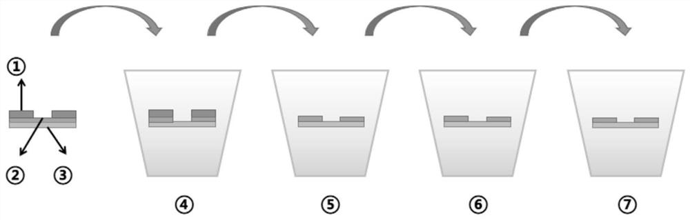
[0021] This embodiment provides a GaSe / MoS based 2 Fabrication process of heterojunction flexible photodetectors. Device structure such as figure 1 As shown, its specific preparation process is as follows:

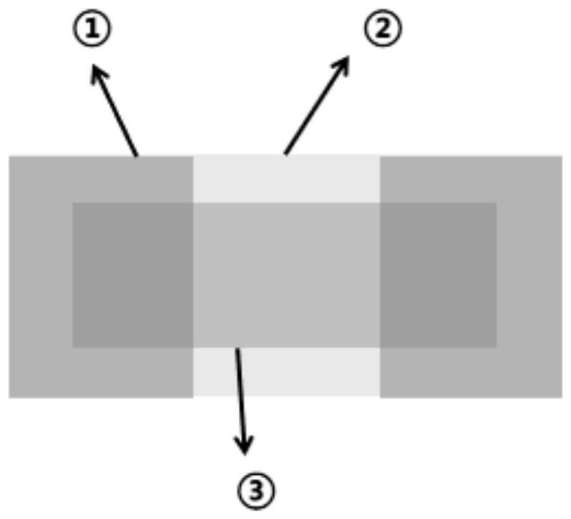
[0022] like figure 2 As shown, ① is 3M tape, ② is rigid substrate, and ③ is PI film covered with ITO. Convert a flexible substrate to a rigid substrate: place the ITO-coated polyimide (PI) film on a rigid substrate, including glass or silicon, and fix it with 3M tape at both ends of the film to ensure that the film is tightly Fixed on a rigid substrate, there is no gap between the film and the rigid substrate, and the middle of the film cannot be covered with tape for subsequent photolithography processing. Compared with methods such as spin-coating pmma as a sacrificial layer, this method is convenient, environmentally friendly, and low in cost.

[0023] Carry out photolithography treatment to described film, comprise utilizing spin coater on film to coat photoresis...


PUM


Abstract

The invention discloses a flexible photoelectric detector based on a selenide/sulfide heterojunction and a preparation method thereof. The sensor adopts a PI film as a substrate, ITO as an electrode, and a heterojunction formed by a P-type selenide with a forbidden band width of 1.2-2.4 eV (such as GaSe with a forbidden band width of about 2.1 eV) and an n-type sulfide with a forbidden band width of 1.8-2.2 eV (such as MoS2 with a forbidden band width of about 1.8 eV) as a functional layer. The preparation method of the flexible photoelectric detector comprises the following steps: firstly, acquiring an ITO electrode through a photoetching technology and ITO wet etching, then acquiring a submicron slice of selenide and sulfide by adopting a mechanical stripping mode, accurately aligning the submicron slice with the ITO electrode, and transferring the submicron slice to the ITO electrode based on a PI substrate to form an ultrathin two-dimensional semiconductor heterojunction (wherein the thickness of each layer is in a range of 10 nm to 30 nm) with an area of a junction region being in a range of 1*10<2> to 2.5*10<3> square microns. The preparation method is convenient, environment-friendly and cheap; the selenide/sulfide heterojunction photoelectric detector prepared based on the method has good bendability, can be applied to more scenes compared with a rigid photoelectric detector, and can be applied to more fields due to the material characteristics of the selenide/sulfide heterojunction; and the photoelectric detector has good photoelectric detection performance and can achieve good photoelectric detection effect.

Description

technical field [0001] The invention belongs to the field of photoelectric sensors and relates to the preparation of a flexible photodetector based on a selenide / sulfide heterojunction. Background technique [0002] With its outstanding performance in fields such as healthcare monitoring and energy harvesting, flexible electronics has attracted widespread attention. It uses a soft substrate instead of the traditional rigid substrate, which can be better shaped and adapted to different substrates, and can still maintain good performance under bending, stretching, etc., and can be used on the surface of the skin, etc., to realize wearable electronic devices , providing a large number of new functions for some practical applications. One of the major trends in the development of wearable devices is the use of flexible photoelectric sensors. High-performance optical detectors play an important role in many fields, and their applications include electro-optical display, photose...

Claims


Application Information

Patent Timeline
Patent Type & Authority Applications(China)
IPC IPC(8): H01L31/0203H01L31/032H01L31/109H01L31/18B82Y30/00B82Y40/00
CPCH01L31/109H01L31/1896H01L31/0203H01L31/032B82Y30/00B82Y40/00Y02P70/50
Inventor 黄文唐雨晴龚天巡林媛张晓升
Owner UNIV OF ELECTRONICS SCI & TECH OF CHINA
Why Eureka
Try Eureka