
Semiconductor packaging antimagnetic structure

A packaging structure, semiconductor technology, applied in the direction of semiconductor devices, semiconductor/solid-state device components, electric solid-state devices, etc., can solve the problems of becoming more and more difficult to be compatible with each other, endangering the health of people around, and electromagnetic pollution.

Pending Publication Date: 2021-07-02
FORMOSA ADVANCED TECH
View PDF0 Cites 0 Cited by
  • Summary
  • Abstract
  • Description
  • Claims
  • Application Information

AI Technical Summary

Problems solved by technology

Moreover, excessive electromagnetic interference will form electromagnetic pollution, endangering the health of people around
With the evolution of equipment and structure, it is becoming more and more difficult to achieve a state of mutual compatibility that can work normally without mutual electromagnetic interference causing performance changes and equipment damage

Method used


Image

  • Semiconductor packaging antimagnetic structure
  • Semiconductor packaging antimagnetic structure
  • Semiconductor packaging antimagnetic structure

Examples


Embodiment Construction

[0013] In order to make the purpose, technical features and advantages of the present invention more understandable to those in the relevant technical field, and to implement the present invention, the technical features and implementation modes of the present invention are specifically explained in conjunction with the attached drawings, and listed The preferred embodiment is further described. The diagrams compared below are intended to express the schematic representations related to the features of the present invention, and are not and need not be completely drawn according to the actual situation. The description about the implementation of this case involves technical content well known to those skilled in the art, and will not be stated again.

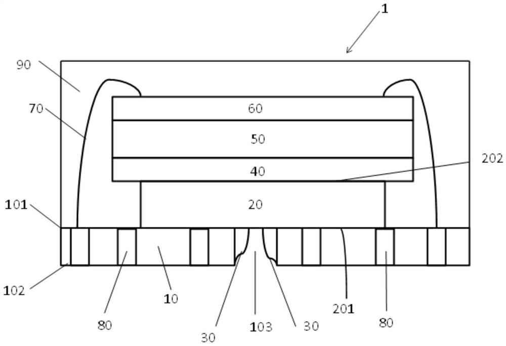
[0014] Please refer to figure 1 , figure 1 It is a schematic diagram of the first embodiment of the antimagnetic structure of the semiconductor package. Such as figure 1 As shown, the semiconductor package antimagnetic stru...


PUM


Abstract

A semiconductor packaging antimagnetic structure is characterized in that the semiconductor packaging antimagnetic structure comprises a substrate, a first chip, a first wire, an adhesive layer, a second chip, a metal film and a second wire; the substrate is provided with an upper surface, a lower surface and a plurality of electric connection structures penetrating through the upper surface and the lower surface, and a window is arranged between the upper surface and the lower surface. The first chip is provided with an active surface and a back surface, the active surface is downwards arranged on the upper surface of the substrate, a part of the active surface of the first chip is exposed in the window, and the part of the active surface exposed in the window is electrically connected with the electric connection structure of the substrate; meanwhile, the first wire electrically connects the active surface with the lower surface of the substrate through the part exposed out of the window. Then, an adhesive layer is arranged on the back face of the first chip, then a second chip is arranged on the adhesive layer, and the second chip is fixed on the back face of the first chip through the adhesive layer. The metal film is arranged on the second chip, and the second wire is electrically connected with the upper surface of the metal film and the upper surface of the substrate at the same time.

Description

technical field [0001] The invention relates to a semiconductor package structure, in particular to a semiconductor package antimagnetic structure. Background technique [0002] Small-sized integrated circuit packaging units are generally built on a single matrix substrate in batches; the matrix substrate pre-defines a plurality of packaging areas, and each packaging area is used to construct a packaging unit. After the encapsulation process is completed, a singulation process can be performed to divide the assembly structure of the encapsulation units constructed on the matrix substrate into individual encapsulation units. The packaging units manufactured in this way include, for example, Thin & Fine Ball Grid Array (TFBGA) packaging units, Quad Flat No-lead (QFN) packaging units, and the like. [0003] Electromagnetic interference is an electromagnetic phenomenon. The electromagnetic waves generated by some electrical and electronic equipment are likely to form electromag...

Claims


Application Information

Patent Timeline
IPC IPC(8): H01L23/552H01L25/18H01L23/31
CPCH01L23/3107H01L23/552H01L25/18
Inventor 姜颖宏林煜能陈政宏
Owner FORMOSA ADVANCED TECH
Features
  • Generate Ideas
  • Intellectual Property
  • Life Sciences
  • Materials
  • Tech Scout
  • Unparalleled Data Quality
  • Higher Quality Content
  • 60% Fewer Hallucinations
Learn More