Preparation method of semiconductor structure and semiconductor structure

A semiconductor and capacitor structure technology, which is applied in semiconductor/solid-state device manufacturing, semiconductor devices, transistors, etc., can solve the problems of large volume, lack of space for dynamic random access memory, and waste of space

Pending Publication Date: 2021-07-06
CHANGXIN MEMORY TECH INC
View PDF11 Cites 2 Cited by
  • Summary
  • Abstract
  • Description
  • Claims
  • Application Information

AI Technical Summary

Problems solved by technology

in the attached Figure 2B In the DRAM unit structure shown, although two sets of capacitors and field effect transistors are arranged alternately, the space occupied is slightly reduced, but it is still arra...

Method used


Image

  • Preparation method of semiconductor structure and semiconductor structure
  • Preparation method of semiconductor structure and semiconductor structure
  • Preparation method of semiconductor structure and semiconductor structure

Examples


Embodiment Construction

[0019] The specific implementations provided by the present invention will be described in detail below in conjunction with the accompanying drawings.

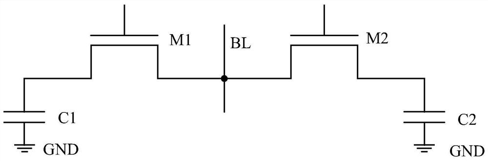
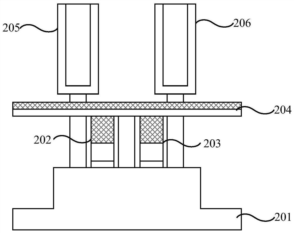
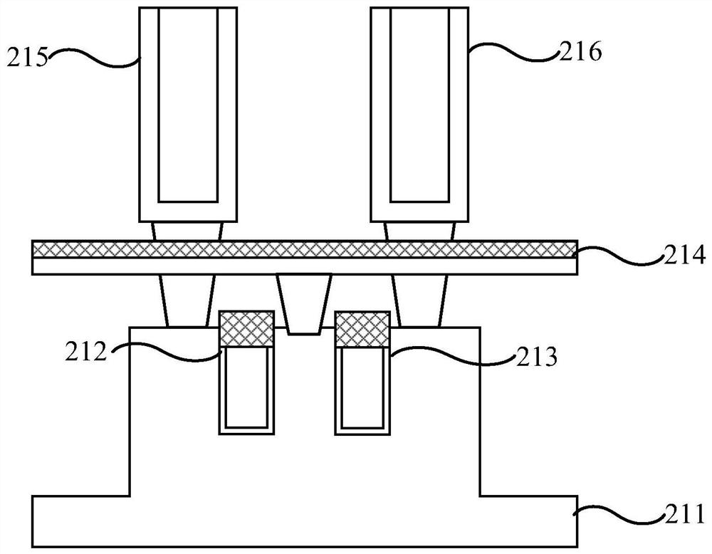
[0020] attached image 3 Shown is a schematic diagram of the steps of the method for preparing a semiconductor structure according to a specific embodiment of the present invention, including: step S30, providing a substrate; step S31, forming a first capacitor structure on the substrate; step S32, forming a first capacitive structure on the first A first transistor structure is formed on the capacitor structure, the source or drain of the first transistor structure is electrically connected to the first capacitor structure; step S33, a bit line structure is formed on the first transistor structure, and the bit line structure is The line structure is electrically connected to the drain or source of the first transistor structure; Step S34, forming a second transistor structure on the bit line structure, the drain or source of ...


PUM


Abstract

The invention provides a preparation method of a semiconductor structure and the semiconductor structure. The method comprises the following steps: providing a substrate; forming a first capacitor structure on the substrate; forming a first transistor structure on the first capacitor structure, wherein a source electrode or a drain electrode of the first transistor structure is electrically connected with the first capacitor structure; forming a bit line structure on the first transistor structure, wherein the bit line structure is electrically connected with a drain electrode or a source electrode of the first transistor structure; forming a second transistor structure on the bit line structure, wherein a drain electrode or a source electrode of the second transistor structure is electrically connected with the bit line structure; and forming a second capacitor structure on the second transistor structure, wherein the second capacitor structure is electrically connected with the source electrode or the drain electrode of the second transistor structure. The vertical gate-all-around field effect transistor is adopted, the size of the semiconductor structure is reduced, more storage units are obtained in the same unit area, and the unit density of the dynamic random access memory is improved.

Description

technical field [0001] The invention relates to the field of semiconductor memory, in particular to a method for preparing a semiconductor structure and the semiconductor structure. Background technique [0002] Due to its excellent cost performance and scalability, dynamic random access memory, as a common volatile memory, is widely used in computing main memory, that is, the most important memory of computers. In the construction process of the DRAM in the prior art, using transistors to control digital signal storage is a common method applied to the DRAM. [0003] Today, as the size of semiconductors shrinks, the storage capacity in the same unit area is getting larger and larger. Improving the unit density of dynamic random access memory (DRAM) is the direction that each generation of product technology has been striving for. Due to Moore's Law, greater integration and relatively smaller DRAM cells have also been a common optimization direction in the industry. In the...

Claims


Application Information

Patent Timeline
IPC IPC(8): H01L21/8242H01L27/108
CPCH10B12/30H10B12/03H10B12/05H10B12/482
Inventor 吴锋
Owner CHANGXIN MEMORY TECH INC
Why Eureka
Try Eureka