Power chip crimping packaging structure and manufacturing method thereof

A packaging structure and power chip technology, which is applied in the fields of printed circuit manufacturing, semiconductor/solid-state device manufacturing, printed circuit assembly of electrical components, etc., can solve problems such as high turn-off speed of unsuitable power chips, achieve low loss and eliminate parasitic parameter, the effect of reducing contact resistance

Pending Publication Date: 2021-07-09
GLOBAL ENERGY INTERCONNECTION RES INST CO LTD +2
View PDF0 Cites 1 Cited by
  • Summary
  • Abstract
  • Description
  • Claims
  • Application Information

AI Technical Summary

Problems solved by technology

[0003] However, at present, most of the packaging structures for high-voltage power chips such as IGBT chips still use the welding package type of silicon-based chips, and its packaging parameters are obviously not suitable for high-voltage power chips such as SiC-based IGBT chips. High turn-off speed, low loss Therefore, it is necessary to develop a new packaging structure for high-voltage power chips

Method used


Image

  • Power chip crimping packaging structure and manufacturing method thereof
  • Power chip crimping packaging structure and manufacturing method thereof
  • Power chip crimping packaging structure and manufacturing method thereof

Examples


Embodiment 1

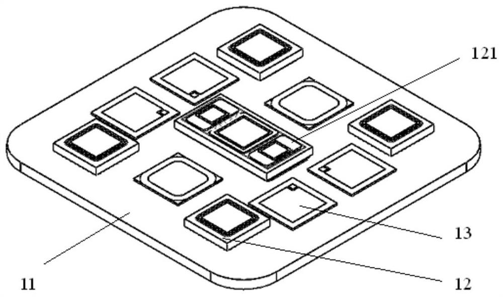
[0040] refer to Figure 1-Figure 10 , this embodiment provides a power chip crimping package structure, including:

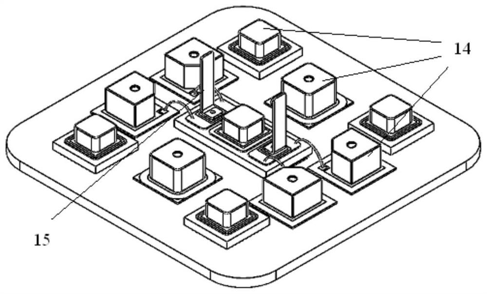
[0041] Base plate 11; multiple IGBT chips 13 and multiple copper-clad ceramic plates 12 are arranged on the base plate 11; each IGBT chip 13 is electrically connected to the copper-clad ceramic plate 12; each IGBT chip 13 and each copper-clad ceramic plate 12 are provided with There are metal pillars 14, and the top surfaces of each metal pillar 14 are located on the same horizontal plane. The material of the metal pillar 14 may be molybdenum-copper alloy or other thermally and electrically conductive metals with a thermal expansion coefficient close to that of the IGBT chip 13 .

[0042] The flexible metal plate 16 , the bottom surface of the flexible metal plate 16 covers and contacts the top surface of each metal column 14 .

[0043] The multi-layer PCB board 18, the multi-layer PCB board 18 is located above the flexible metal plate 16, and the multi-layer ...

Embodiment 2

[0062] refer to Figure 1-Figure 10 , the present embodiment provides a method for manufacturing a power chip crimping package structure, including the following steps:

[0063] refer to figure 1 , providing a bottom plate 11;

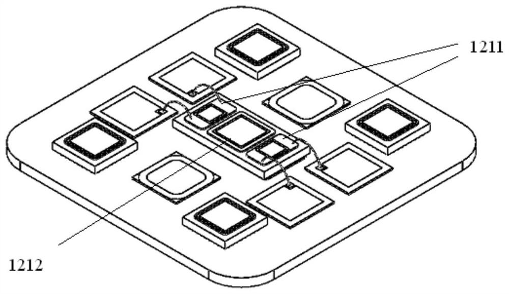
[0064] refer to figure 2 , welding a plurality of IGBT chips 13 and a plurality of copper-clad ceramic plates 12 on the base plate 11; each IGBT chip 13 is electrically connected to the copper-clad ceramic plate 12;

[0065] refer to image 3 , metal pillars 14 are formed on each IGBT chip 13 and each copper-clad ceramic plate 12, and the top surfaces of each metal pillar 14 are located on the same horizontal plane;

[0066] refer to Figure 4 , the flexible metal plate 16 is set, the bottom surface of the flexible metal plate 16 covers and contacts the top surface of each metal column 14; a plurality of auxiliary emitter lead-out terminals 161 are set on the top surface of the flexible metal plate 16;

[0067] refer to Image 6 , the multilay...

Embodiment 3

[0074] refer to Figure 11-Figure 20 , this embodiment provides another power chip crimping package structure, including:

[0075] Base plate 21; multiple IGBT chips 231 and multiple copper-clad ceramic plates 22 are arranged on the base plate 21; each IGBT chip 231 is electrically connected to the copper-clad ceramic plate 22; each IGBT chip 231 and each copper-clad ceramic plate 22 are provided with There are metal pillars 24, and the top surfaces of each metal pillar 24 are located on the same horizontal plane. The material of the metal pillar 24 may be molybdenum-copper alloy or other thermally and electrically conductive metals with a thermal expansion coefficient close to that of the IGBT chip 231 .

[0076] The flexible metal plate 26 , the bottom surface of the flexible metal plate 26 covers and contacts the top surface of each metal post 24 .

[0077] The multilayer PCB board 28 , the multilayer PCB board 28 is located above the flexible metal plate 26 , and the mul...


PUM


Abstract

The invention discloses a power chip crimping packaging structure and a manufacturing method thereof. The power chip crimping packaging structure comprises a bottom plate, and the bottom plate is provided with a plurality of IGBT chips and a plurality of copper-clad ceramic plates. Each IGBT chip and each copper-clad ceramic plate are respectively provided with a metal column, and the top surfaces of the metal columns are located on the same horizontal plane. The bottom surface of a flexible metal plate covers and is in contact with the top surfaces of the metal columns; a plurality of auxiliary emitting electrode leading-out terminals are arranged on the top surface of the flexible metal plate, and the auxiliary emitting electrode leading-out terminals are electrically contacted with the flexible metal plate; a multi-layer PCB is positioned above the flexible metal plate, and the multi-layer PCB is electrically contacted with the plurality of auxiliary emitting electrode leading-out terminals; the multi-layer PCB is provided with a through hole penetrating through the multi-layer PCB; and an emitter electrode is located above the multi-layer PCB, the emitter electrode is provided with a plurality of crimping arms, and the plurality of crimping arms penetrate through the through holes of the multi-layer PCB to be crimped with the flexible metal plate.

Description

technical field [0001] The invention relates to the field of power device packaging, in particular to a power chip crimping packaging structure and a manufacturing method thereof. Background technique [0002] At present, the vast majority of high-power power electronic devices in power systems use silicon power electronic devices, such as IGBT (Insulated Gate Bipolar Transistor, insulated gate bipolar transistor) chip devices, thyristor chip devices, GTO (Gate Turn-Off thyristor, Thyristor) chip devices can be turned off to realize the control and conversion of electric energy. Since silicon power electronic devices are limited by the physical characteristics of the material itself such as withstand voltage and operating temperature, it is necessary to fundamentally improve the high-power power electronic equipment. To improve the reliability and stability of the system, reduce the overall loss of the system, and improve the control conversion efficiency of energy, it is ne...

Claims


Application Information

Patent Timeline
Patent Type & Authority Applications(China)
IPC IPC(8): H01L25/07H01L23/373H01L21/60H05K3/30H05K1/18
CPCH01L23/3736H01L24/81H01L25/072H05K1/182H05K3/301
Inventor 王亮石浩孙帅陈陶胡婷婷
Owner GLOBAL ENERGY INTERCONNECTION RES INST CO LTD
Why Eureka
Try Eureka