Supercharge Your Innovation With Domain-Expert AI Agents!

IGBT layout structure

A technology of layout structure and pressure solder joints, applied in the direction of electrical components, electrical solid devices, circuits, etc., can solve the problems that the probe station cannot be realized, and achieve the effect of facilitating testing and reducing requirements

Pending Publication Date: 2021-07-09
上海埃积半导体有限公司
View PDF0 Cites 1 Cited by
  • Summary
  • Abstract
  • Description
  • Claims
  • Application Information

AI Technical Summary

Problems solved by technology

The IGBT device has three electrodes, which are the collector C (Collector), the gate G (Gate), and the emitter E (Emmiter). IGBT, like many other power devices, in order to be able to withstand high enough voltage per unit area Blocking the voltage and being able to switch as much current as possible, the device is generally designed as a vertical structure, that is, the collector C is located on the back of the chip, and the gate G and emitter E are located on the front of the chip. The schematic diagram of the conventional IGBT layout design is as follows figure 1 As shown, when performing chip-level testing, it is necessary to press the electrode on the back of the chip, which is impossible for many probe stations without tray pressurization capabilities.

Method used


Image

  • IGBT layout structure
  • IGBT layout structure
  • IGBT layout structure

Examples


Embodiment 1

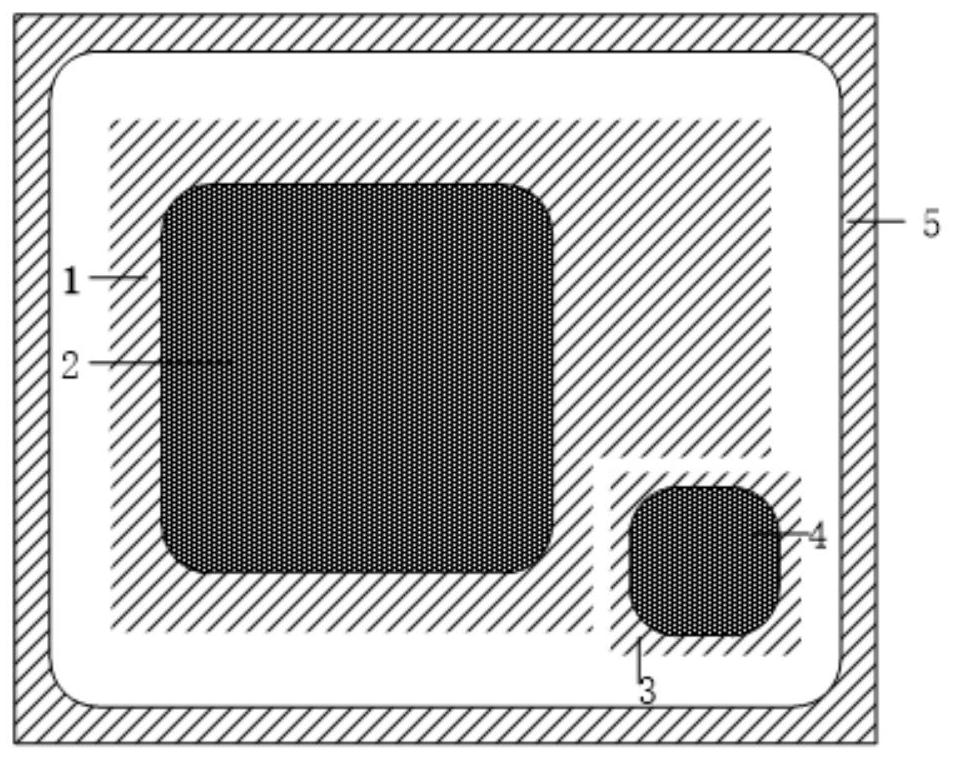
[0026] This embodiment discloses an IGBT layout structure, such as figure 2 As shown, it includes: a cell area 7, and a terminal metal ring 5 located at the outer circle of the cell area; an emitter metal 1 and an emitter electrically connected to the emitter metal 1 are arranged on the cell area 7 Extreme pressure pad 2, grid metal 3 and grid pad 4 electrically connected to the gate metal 3; at least one collector pad 6 is also provided on the terminal metal ring 5; the terminal The areas of the non-collector voltage solder joints on the metal ring 5 are all covered by the passivation layer.

[0027] The collectors of conventional IGBTs are generally set on the back of the chip, and the gate and emitter are set on the front of the chip. However, in this embodiment, on the basis of the conventional IGBT layout structure, additional collector pressure pads are added on the front of the layout (the back structure of the IGBT in this application is the same as that of the conve...

Embodiment 2

[0039] In this embodiment, on the basis of the first embodiment, there are a plurality of collector pads, which are evenly distributed on the terminal metal ring.

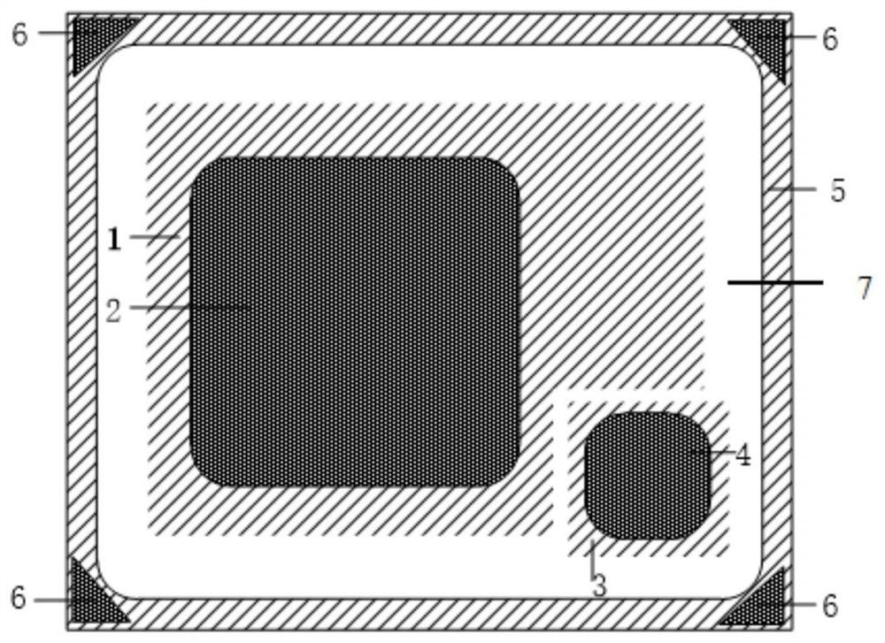
[0040] Preferably, the terminal metal ring is a rectangular ring, and the collector pads are arranged at corners of the terminal metal ring. The number of the collector voltage soldering points is not more than 4. For example, one, or 2, or 3, or 4 collector voltage soldering points can be arranged on the terminal metal ring of the front layout of the IGBT. In addition, the collector pads are arranged at the corners of the rectangular metal ring, and no more than one pad is provided at each corner. like Figure 5 As shown, in the front layout structure of the IGBT, only one collector voltage solder joint is set at the corner of the terminal metal ring. Of course, it is best to set a collector voltage soldering point at each corner, so that in the subsequent test, there is no need to locate the corner where the co...

Embodiment 3

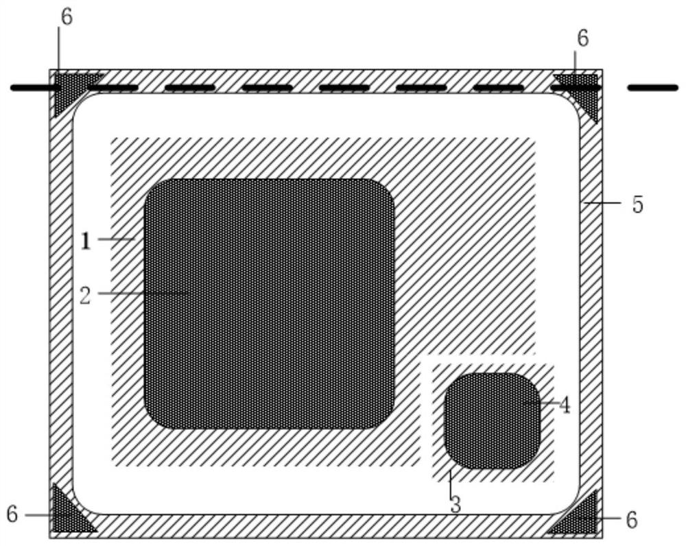
[0045] Technical solutions such as figure 2 Shown: The layout diagram includes the emitter metal layer 1, the emitter pad 2 located on the emitter metal (the emitter metal at the emitter pad 2 is exposed, and the rest of the area is covered by the passivation layer), the gate The pole metal layer 3 is located on the gate pad 4 above the gate metal (the gate metal layer 3 is exposed except the gate metal at the gate pad 4, and the rest of the area is covered by a passivation layer), located on The terminal metal ring 5 on the edge of the chip and the collector pressure pad 6 above the terminal metal ring 5 (the area at the collector pressure pad 6 is the exposed metal layer on the terminal metal ring, and the rest of the terminal metal ring is passivated Layer coverage), the shape of the collector pressure pad 6 includes but is not limited to Image 6 As shown in the triangle, square, rectangle, etc., in the IGBT front layout structure of this embodiment, one collector pressu...


PUM


Abstract

The invention discloses an IGBT layout structure. The IGBT layout structure comprises a cellular area and a terminal metal ring positioned on the outer circle of the cellular area, wherein the cellular area is provided with emitter metal, an emitter pressure welding point electrically connected with the emitter metal, gate metal and a gate pressure welding point electrically connected with the gate metal; the terminal metal ring is also provided with at least one collector electrode pressure welding point; and non-collector pressure welding spot areas on the terminal metal ring are covered by a passivation layer. By adopting the IGBT layout structure provided by the invention, the parameters of an IGBT chip can be tested under the condition that the back surface of the IGBT chip does not need to be pressurized, and requirements on a probe station of chip test equipment is reduced.

Description

technical field [0001] The invention relates to the field of power components, in particular to an IGBT layout structure. Background technique [0002] IGBT (Insulated Gate Bipolar Transistor), Insulated Gate Bipolar Transistor, is a composite fully-controlled voltage-driven power semiconductor device composed of BJT (Bipolar Transistor) and MOS (Insulated Gate Field Effect Transistor), with MOSFET The advantages of high input impedance and low conduction voltage drop of BJT. The IGBT device has three electrodes, which are the collector C (Collector), the gate G (Gate), and the emitter E (Emmiter). IGBT, like many other power devices, in order to be able to withstand high enough voltage per unit area Blocking the voltage, and being able to switch as much current as possible, the device is generally designed as a vertical structure, that is, the collector C is located on the back of the chip, and the gate G and emitter E are located on the front of the chip. The schematic di...

Claims


Application Information

Patent Timeline
Patent Type & Authority Applications(China)
IPC IPC(8): H01L27/02H01L29/739
CPCH01L27/0207H01L29/7393
Inventor 程炜涛姚阳
Owner 上海埃积半导体有限公司
Features
  • R&D
  • Intellectual Property
  • Life Sciences
  • Materials
  • Tech Scout
  • Unparalleled Data Quality
  • Higher Quality Content
  • 60% Fewer Hallucinations
Learn More