

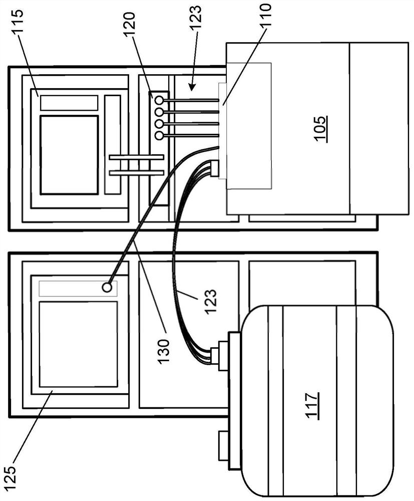
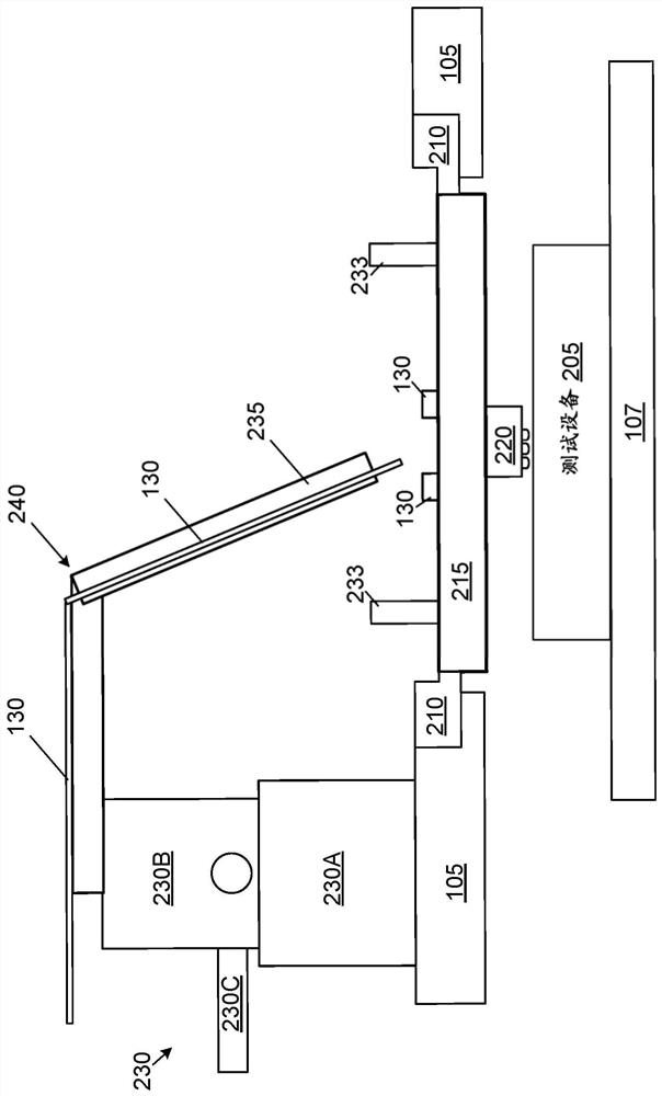
Compact opto-electric probe
A photodetector and optoelectronic technology, applied in the field of optical and electrical interface systems, can solve problems such as difficult mixing of optical and electrical wafer wafer level testing
- Summary
- Abstract
- Description
- Claims
- Application Information
AI Technical Summary
Problems solved by technology
Method used
Image

Examples
example 1
[0045] Example 1. A photodetector for interfacing with an optoelectronic device, the photodetector comprising: an electrical layer having electrical paths, at least some of which are connected to electrical terminals configured to interface with the optoelectronic an electrical component of the device is interfaced, the electrical path avoiding the optical path formed in the electrical layer; and an optical interface is used to interface with the optical component of the optoelectronic device, the optical interface is arranged to pass through the optical path formed in the electrical layer and Optical components for optical communication.
example 2
[0046] Example 2. A photodetector according to example 1 comprising a flexible optical fiber to allow positioning of the photodetector into an operative position in which the electrical terminals are in electrical contact with the electrical contacts of the optoelectronic device and the optical interface is in contact with Optical components are optically aligned.
example 3
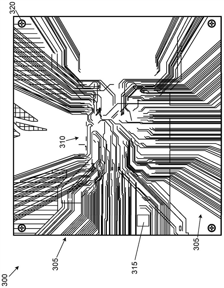
[0047] Example 3. The photodetector according to any one of examples 1 or 2, wherein the electrical layer comprises a film comprising electrical paths, and wherein the electrical terminals extend from the film to corresponding electrical contacts of the optoelectronic device.
PUM
| Property | Measurement | Unit |
|---|---|---|
| radius | aaaaa | aaaaa |
Abstract
Description
Claims
Application Information