Wet etching method for electrode metal layer of silicon carbide device

A wet etching, metal layer technology, applied in semiconductor/solid-state device manufacturing, circuits, electrical components, etc., can solve the problem of poor etching uniformity at the edge of the die, affecting the electrical performance of silicon carbide devices. Product qualification rate and etching rate There are big differences and other problems to achieve the effect of shortening the etching process time, improving the etching uniformity, and improving the electrical performance and yield.

Pending Publication Date: 2021-07-16
ZHUZHOU CRRC TIMES SEMICON CO LTD
View PDF0 Cites 0 Cited by
  • Summary
  • Abstract
  • Description
  • Claims
  • Application Information

AI Technical Summary

Problems solved by technology

In the tank body immersion etching method, due to many reasons such as vertical shaking of the robot arm and etching bubbles, the etching rate of the same silicon carbide wafer is very different in the horizontal direction (X direction) and vertical direction (Y direction). (X direction) or vertical direction (Y direction) there is a large area of ​​etching residue, especially the etching uniformity at the edge of the die is very poor, which will eventually affect the electrical performance of silicon carbide devices and the yield of products

Method used


Image

  • Wet etching method for electrode metal layer of silicon carbide device
  • Wet etching method for electrode metal layer of silicon carbide device

Examples


Embodiment Construction

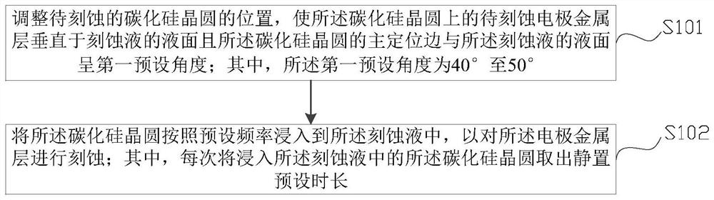
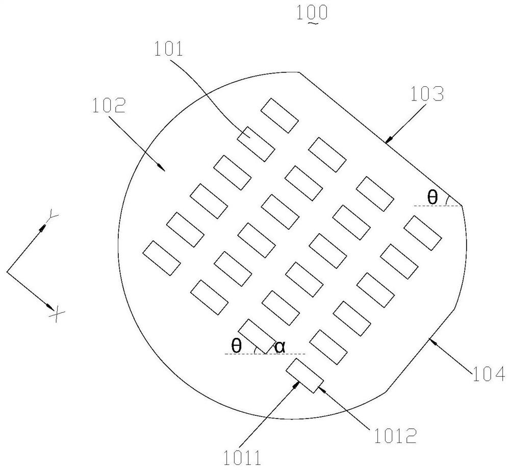
[0022] The implementation of the present disclosure will be described in detail below in conjunction with the accompanying drawings and embodiments, so as to fully understand and implement the realization process of how to apply technical means to solve technical problems and achieve corresponding technical effects in the present disclosure. The embodiments of the present disclosure and the various features in the embodiments can be combined with each other under the premise of no conflict, and the formed technical solutions are all within the protection scope of the present disclosure. In the drawings, the size and relative sizes of layers and regions may be exaggerated for clarity. Like reference numerals refer to like elements throughout.

[0023] The terminology used herein is for the purpose of describing particular embodiments only and is not to be taken as a limitation of the present disclosure. As used herein, the singular forms "a", "an" and "the / the" are intended to...


PUM

PropertyMeasurementUnit
Thicknessaaaaaaaaaa

Abstract

The invention provides a wet etching method for an electrode metal layer of a silicon carbide device. The method comprises the steps that the position of a silicon carbide wafer to be etched is adjusted, so that an electrode metal layer to be etched on the silicon carbide wafer is perpendicular to the liquid level of etching liquid, and a first preset angle is formed between the main positioning edge of the silicon carbide wafer and the liquid level of the etching liquid, and the first preset angle ranges from 40 degrees to 50 degrees; the silicon carbide wafer is immersed into the etching liquid according to a preset frequency so as to etch the electrode metal layer; wherein each time the silicon carbide wafer immersed in the etching liquid is taken out, the silicon carbide wafer is subjected to standing for a preset period of time. The etching difference of each tube core in the longitudinal direction and the transverse direction in the etching process of the electrode metal layer can be eliminated, hydrogen bubbles which are generated in the etching process of the electrode metal layer and are attached to the surface of the electrode metal layer can be eliminated, and etching residues are avoided. The electrical property and the yield of the device are improved, and the manufacturing cost is saved.

Description

technical field [0001] The present disclosure relates to the technical field of semiconductor devices, in particular to a wet etching method for an electrode metal layer of a silicon carbide device. Background technique [0002] Silicon carbide material has the advantages of wide bandgap, high thermal conductivity, high breakdown field strength, high saturation velocity, etc. The power device manufactured by it can greatly exert its high temperature, high frequency and low loss characteristics, making it in high voltage, High temperature, high frequency, high power, strong radiation and other aspects have great application prospects. [0003] In the manufacturing process of silicon carbide devices, the wet etching methods of the electrode metal layer on the silicon carbide wafer mainly include rotary spraying and tank immersion. In the tank body immersion etching method, due to many reasons such as vertical shaking of the robot arm and etching bubbles, the etching rate of t...

Claims


Application Information

Patent Timeline
IPC IPC(8): H01L21/04
CPCH01L21/0445H01L21/048
Inventor 刘启军马亚超刘锐鸣赵艳黎周正东刘芹黄爱权李诚瞻
Owner ZHUZHOU CRRC TIMES SEMICON CO LTD
Why Eureka
Try Eureka