Detection device for detecting thickness of semiconductor wafer

A detection device and semiconductor technology, applied in measuring devices, cleaning methods using gas flow, transportation and packaging, etc., can solve the problem that the detection device cannot be quickly positioned, reduce the risk of scratches, improve the convenience of use, The effect of reducing misalignment

Active Publication Date: 2021-07-30
江苏振宁半导体研究院有限公司
View PDF6 Cites 3 Cited by
  • Summary
  • Abstract
  • Description
  • Claims
  • Application Information

AI Technical Summary

Problems solved by technology

[0006] The purpose of the present invention is to provide a detection device for detecting the thickness of a semiconductor wafer, to solve the problem that the above-mentioned semiconductor wafer detection device cannot be quickly positioned

Method used


Image

  • Detection device for detecting thickness of semiconductor wafer
  • Detection device for detecting thickness of semiconductor wafer
  • Detection device for detecting thickness of semiconductor wafer

Examples


Embodiment Construction

[0032] The present invention will be described in detail below in conjunction with various embodiments shown in the drawings. However, these embodiments do not limit the present invention, and structural, method, or functional changes made by those skilled in the art according to these embodiments are included in the protection scope of the present invention.

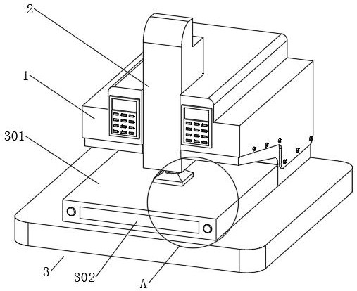
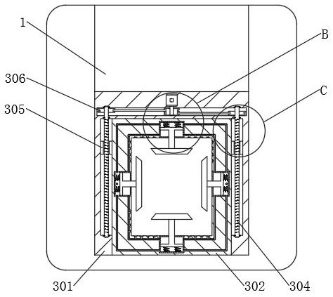
[0033] The invention discloses a detection device for detecting the thickness of a semiconductor wafer. Figure 1-Figure 7 As shown, it includes a detection device body 1 , a detection mechanism 2 , a moving conveying mechanism 3 , and a positioning mechanism 4 .

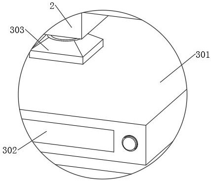
[0034] ginseng figure 1 As shown, the detection mechanism 2 is arranged on one side of the detection device body 1 , so that the thickness detection of the detection device body 1 is facilitated by the detection mechanism 2 .

[0035] ginseng figure 1 As shown, the moving conveying mechanism 3 is arranged between the detecting mechanism 2 and the detecting...


PUM


Abstract

The invention discloses a detection device for detecting the thickness of a semiconductor wafer. The detection device comprises a detection device body, a detection mechanism, a movable conveying mechanism and a positioning mechanism, wherein the detection mechanism is arranged on one side of the detection device body; the movable conveying mechanism is arranged between the detection mechanism and the detection device body, and the movable conveying mechanism comprises a carrying box, wherein a movable carrying disc is arranged in the carrying box; and the positioning mechanism is arranged in the movable carrying disc and comprises a plurality of movable positioning plates. The detection device for detecting thickness of semiconductor wafer is additionally provided with corresponding mechanisms, so that the semiconductor wafer can be automatically positioned, the use convenience of the detection device for detecting thickness of the semiconductor wafer is remarkably improved, the deviation condition of the semiconductor wafer in the detection process is reduced, the detection accuracy of the detection device for detecting thickness of the semiconductor wafer is greatly improved, and the risk that the semiconductor wafer is scratched in the detection process of the detection device for detecting thickness of the semiconductor wafer is reduced.

Description

technical field [0001] The invention belongs to the technical field of semiconductor wafer detection devices, and in particular relates to a detection device for detecting the thickness of a semiconductor wafer. Background technique [0002] Semiconductor wafer is a kind of semiconductor light-emitting component composed of semiconductor materials. Semiconductor wafer is the main raw material of LED and the core component of LED light-emitting. During the manufacturing process of semiconductor wafer, it is necessary to control the brightness, voltage, wavelength, length, thickness, Parameters such as width are detected. [0003] In the semiconductor wafer inspection process, a thickness detection device needs to be used to detect the thickness of the center point of the semiconductor wafer. According to different detection methods, the semiconductor thickness detection device can be divided into: contact thickness detection device and non-contact thickness detection device. ...

Claims


Application Information

Patent Timeline
Patent Type & Authority Applications(China)
IPC IPC(8): G01B21/08B65G49/06B65G47/22B08B5/02
CPCB08B5/02B65G47/22B65G49/06G01B21/08
Inventor 张硕柯海丰
Owner 江苏振宁半导体研究院有限公司
Why Eureka
Try Eureka