Silicon-based eutectic bonding structure, micro-mechanical device, packaging structure and preparation method

A technology of micromechanical devices and eutectic bonding, which is applied in the direction of optomechanical equipment, microstructure devices, metal processing machinery parts, etc., can solve the problems that hinder the reliable formation of bonding structures, and achieve the improvement of mechanical bonding reliability and electrical Interconnect contact reliability, broadening the effect of device fabrication

Active Publication Date: 2021-08-03
SOUTH CHINA AGRI UNIV
View PDF13 Cites 0 Cited by
  • Summary
  • Abstract
  • Description
  • Claims
  • Application Information

AI Technical Summary

Problems solved by technology

In this case, if Au-Si, Al-Si and other silicon-based eutectic bonding technologies also need to build local electrical contacts (such as forming metal / semiconductor contacts) and local electrical contacts between the eutectic bonding metal and the silicon wafer body. The isolation region is used to form the electrical interconnection structure of the eutectic bonding layer, and a step introduced by the insulating layer will be generated between the bonding metal medium of the silicon-based eutectic reaction and the silicon body to form a certain height difference, while The existence of the height difference restricts the liquid phase flow channel formed by the metal / bulk silicon eutectic reaction to the edge of the step introduced by the insulating layer, which will hinder the reliable formation of the bonding structure based on the silicon-based eutectic reaction

Method used


Image

  • Silicon-based eutectic bonding structure, micro-mechanical device, packaging structure and preparation method
  • Silicon-based eutectic bonding structure, micro-mechanical device, packaging structure and preparation method
  • Silicon-based eutectic bonding structure, micro-mechanical device, packaging structure and preparation method

Examples


Embodiment 1

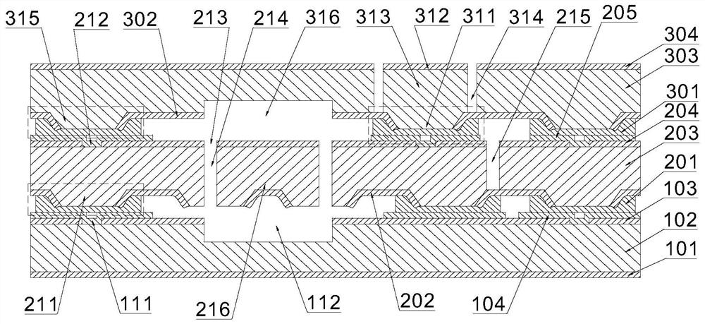
[0051] see figure 1 , the micromechanical device adopting the silicon-based eutectic bonding structure in this embodiment includes a device silicon wafer 203, and both sides of the device silicon wafer 203 are sequentially provided with a device insulating layer 202 and a device-side bonding metal layer 201, Wherein, the device insulating layer 202 at the bottom side is provided with a device bottom side insulating layer window, and the device side bonding metal layer 201 at the bottom side is in electrical contact with the device silicon wafer 203 through the device bottom side insulating layer window; The device-side bonding metal layer 201 and the substrate-side bonding metal layer 104 are connected to each other to form a bonding structure; the silicon wafer 203 of the device is provided with a silicon boss 211 at a position corresponding to the window of the insulating layer on the bottom side of the device, The silicon boss 211 is surrounded by an insulating layer, and t...

Embodiment 2

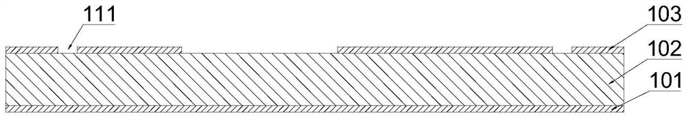
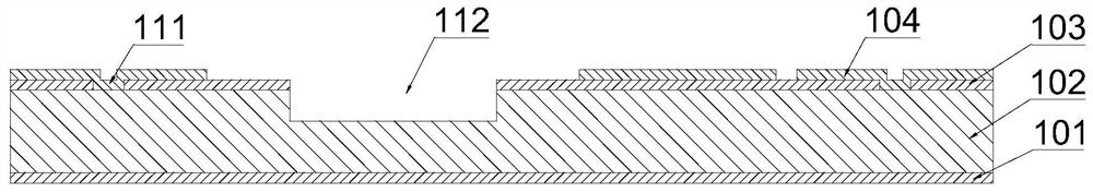
[0067] see figure 1 , the silicon-based eutectic bonding micromechanical packaging structure in this embodiment includes a micromechanical device and a cover plate packaging interconnection structural unit, the micromechanical device includes a substrate unit and a device unit, and the substrate unit It includes a substrate silicon wafer 102 on which a substrate insulating layer 103 and a substrate-side bonding metal layer 104 are sequentially disposed.

[0068] The cover package interconnection structure unit includes a cover silicon chip 303, the bottom side of the cover silicon chip 303 is provided with a cover insulating layer 302 and a cover side bonding metal layer 301 in turn, and the cover silicon chip 303 The top side is provided with a cover plate top side metal layer 304; wherein, the cover plate side bonding metal layer 301 is bonded to the device side bonding metal layer 201 through a silicon-based eutectic bonding structure including the silicon boss 211 The cov...


PUM


Abstract

The invention discloses a silicon-based eutectic bonding structure, a micro-mechanical device, a packaging structure and a preparation method. The silicon-based eutectic bonding structure comprises a silicon boss wrapped in an insulating layer, wherein the surface height of the silicon boss is higher than or equal to the surface height of the insulating layer located at the bottom part of the silicon boss. A device unit in the micro-mechanical device is in bonding connection with a substrate unit through the silicon-based eutectic bonding structure, and an electrode of a substrate silicon wafer is led out to a device silicon wafer through the silicon-based eutectic bonding structure. The silicon boss structure is formed by using a silicon local oxidation method, a silicon region of the device is exposed, and etching penetration of a movable structure of the device is ensured. A cover plate packaging interconnection structure unit in the micro-mechanical packaging structure is mechanically and electrically connected by bonding a silicon-based eutectic bonding structure and a micro-mechanical device. According to the silicon-based eutectic bonding structure, the surface height of the silicon boss is higher than or equal to the surface height of the insulating layer by regulating and controlling the thickness of a silicon local oxide layer twice, and the mechanical connection reliability and the electrical contact reliability of the silicon-based eutectic bonding structure are improved.

Description

technical field [0001] The invention relates to a micromechanical device, a packaging structure and a preparation method, in particular to a silicon-based eutectic bonding structure, a micromechanical device, a packaging structure and a preparation method. Background technique [0002] Micro Electro Mechanical System (MEMS) is a general term for micromechanical components formed on silicon or other dielectric wafers through semiconductor technology and micro-nano processing technology, and finally integrated with signal processing circuits. Wafer bonding technology is a key technology for MEMS device manufacturing and packaging. The main wafer bonding technologies include silicon-silicon fusion bonding, silicon-glass anode bonding, glass paste bonding, polymer bonding, and eutectic bonding. , diffusion bonding, etc. Different bonding technologies have their limitations, but silicon-silicon bonding (bonding temperature is about 600-1200°C high, high wafer surface quality req...

Claims


Application Information

Patent Timeline
Patent Type & Authority Applications(China)
IPC IPC(8): B81C3/00B81C1/00B81B7/02B81B7/00
CPCB81B7/02B81C3/001B81C1/00301B81B7/0006B81C2203/033
Inventor 梁亨茂
Owner SOUTH CHINA AGRI UNIV
Why Eureka
Try Eureka