Monolithic ceramic electronic element and its producing method

A technology of ceramic electronic components and monoliths, which is applied in the field of monolithic ceramic electronic components and its manufacturing, to achieve the effects of simple process, reduced thickness and shortened process time

Inactive Publication Date: 2003-12-24
MURATA MFG CO LTD
View PDF1 Cites 0 Cited by
  • Summary
  • Abstract
  • Description
  • Claims
  • Application Information

AI Technical Summary

Problems solved by technology

[0017] The second method encounters the problem that the thickness of the part with internal electrodes covering each other is thicker than the thickness of the part without internal electrodes
However, this requirement cannot be easily met by

Method used


Image

  • Monolithic ceramic electronic element and its producing method
  • Monolithic ceramic electronic element and its producing method
  • Monolithic ceramic electronic element and its producing method

Examples


Embodiment 1

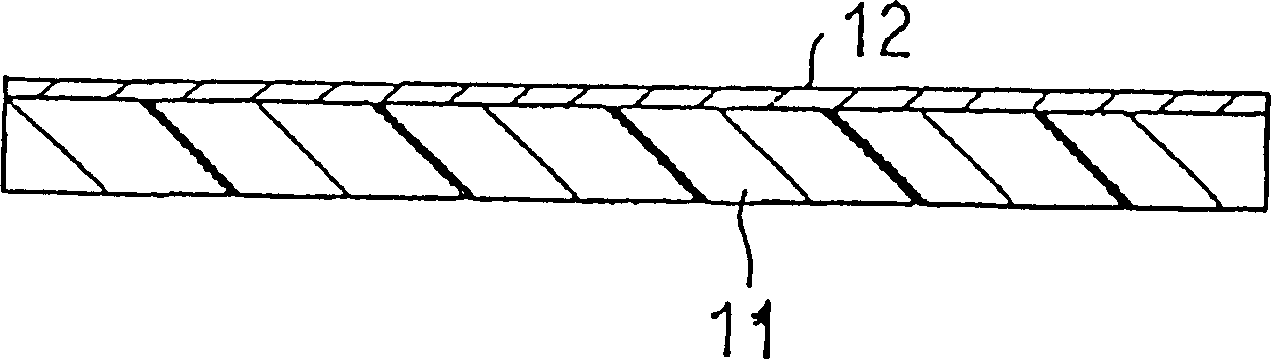
[0070] As shown in FIG. 3A, a polyethylene terephthalate film 11 serving as a first support member is coated with a silicone resin (not shown). Next, the first metal film 12 is formed on the polyethylene terephthalate film 11 . On the entire surface of the film 11, a first-layer metal film 12 composed of an Ag (silver) layer is formed to a thickness of 0.1 µm by evaporation.

[0071] Afterwards, a photoresist is added on the first metal film layer 12 to form a photoresist layer 13 with a thickness of 0.8 μm. The main component of the photoresist is BaTio containing 10vol% 3 Powdered quinone and diazide-based formalin resins.

[0072] Then, exposure and development processes are performed to obtain the photoresist layer 13 in which pattern holes 13a are formed as shown in FIG. 3B.

[0073] Thereafter, the second metal film 14 is formed on the first metal film 12 in the region of the patterned hole 13a formed in the photoresist layer 13 . Pd was applied by electroplating to ...

no. 2 Embodiment

[0084] A multilayer ceramic substrate is produced in a manner similar to that of the first embodiment, except that a copper (Cu) film is used instead of a silver (Ag) film as the first metal film, and a Ni film is used instead of a Pd film as the second metal film. The resist resin contains 10vol% Al 2 o 3 powder, and 5vol% glass powder, and sintered at 1200°C in a reducing atmosphere.

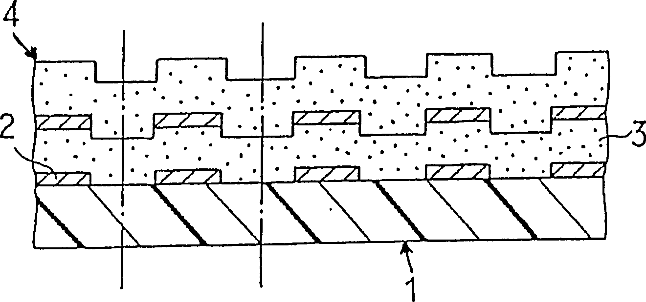
[0085] In the obtained multilayer ceramic substrate, the formation of a stepped portion between the portion where the internal electrodes overlap each other and the portion where the internal electrodes do not overlap each other is prevented.

[0086] The properties of the obtained multilayer ceramic substrates were tested. As a result, the characteristics of the design are obtained. The obtained multilayer ceramic substrate was cut in its thickness direction. As a result, no defects due to delamination were found.

[0087] The region where the photoresist layer is formed is in substantia...

no. 3 Embodiment

[0090] Monolithic capacitors were fabricated in a manner similar to that of Example 1, except that inorganic powders such as ceramic powder and glass powder were not added to the photoresist used.

[0091] The step portion between the portion where the internal electrodes overlap each other and the portion where the internal electrodes do not overlap each other cannot be sufficiently reduced. However, uniform pressurization in the pressurization process after the stacking process satisfactorily prevents delamination as compared with monolithic capacitors obtained by conventional methods.

[0092] Although the first metal film and the second metal film are formed of different metals in the structures of the first to third embodiments, the first metal film and the second metal film may be formed of the same metal.


PUM

PropertyMeasurementUnit
Thicknessaaaaaaaaaa
Thicknessaaaaaaaaaa
Thicknessaaaaaaaaaa

Abstract

A method of manufacturing a monolithic ceramic electronic device includes the following steps: forming a first metal film on a PET film; forming a multilayered metal film by forming a second metal film on a part of the first metal film; forming a monolithic ceramic structure including the multilayered metal film; forming a portion of the first metal film into an insulating structure and firing the ceramics. Disclosed also is a monolithic ceramic electronic device manufactured by the method. As a result, a stepped portion between a portion in which the internal electrodes overlap one another and a portion in which the internal electrodes do not overlap can be prevented from being formed, generation of delamination can effectively be prevented.

Description

technical field [0001] The invention relates to an electronic component and a manufacturing method thereof, in particular to a monolithic ceramic electronic component and a manufacturing method thereof. [0002] The present invention is suitable for various electronic components, for example, monolithic capacitors, monolithic piezoelectric elements or multilayer ceramic substrates, and methods of manufacturing these components. Background technique [0003] Monolithic ceramic electronic components, such as monolithic capacitors with internal electrodes, have been manufactured by integrally sintering metal and ceramic components. Firstly, conductive paste patterns are printed on the ceramic green sheets to form internal electrodes, and then a plurality of ceramic green sheets with internal electrodes are stacked. Then, an appropriate number of ceramic green sheets without internal electrodes are stacked on both sides of the stack of ceramic green sheets stacked in this way t...

Claims


Application Information

Patent Timeline
IPC IPC(8): H01G4/30H01L21/48H05K1/03H05K3/10H05K3/20H05K3/46
CPCH05K3/205H05K3/4611H05K2203/0315H01L21/4857Y10T29/49163H05K2203/1142H01G4/308H05K2203/0156H05K1/0306H05K3/108H05K3/4629H01G4/12
Inventor 川上博之河野芳明久保寺纪之
Owner MURATA MFG CO LTD
Why Eureka
Try Eureka