Stack type micro-display driving chip architecture and preparation method thereof

A display driver and stacking technology, applied to static indicators, instruments, etc., can solve the problems of limiting the performance improvement of micro-display driver ICs, incompatibility, and difficulty in integration, etc., to meet large drive currents, solve poor compatibility, and improve good performance. rate effect

Pending Publication Date: 2021-08-06
ANHUI SEMICON INTEGRATED DISPLAY TECH CO LTD
View PDF0 Cites 3 Cited by
  • Summary
  • Abstract
  • Description
  • Claims
  • Application Information

AI Technical Summary

Problems solved by technology

However, due to differences in manufacturing processes, it is difficult to integrate processes with a large gap on the same wafer. For example, it is possible to integrate 0.5um and 0.18um processes on the same wafer, but it is difficult to integrate 0.5um and 45nm processes. This process Incompatibility greatly limits the performance improvement of micro-display driver ICs, so it is meaningful to reduce costs and develop high-performance micro-display driver ICs

Method used


Image

  • Stack type micro-display driving chip architecture and preparation method thereof
  • Stack type micro-display driving chip architecture and preparation method thereof
  • Stack type micro-display driving chip architecture and preparation method thereof

Examples


Embodiment Construction

[0024] Referring to the accompanying drawings, through the description of the embodiments, the specific embodiments of the present invention include the shape, structure, mutual position and connection relationship of each part, the function and working principle of each part, and the manufacturing process of the various components involved. And the method of operation and use, etc., are described in further detail to help those skilled in the art have a more complete, accurate and in-depth understanding of the inventive concepts and technical solutions of the present invention.

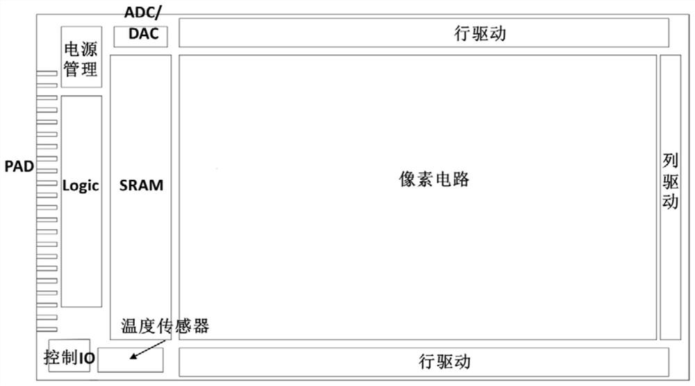
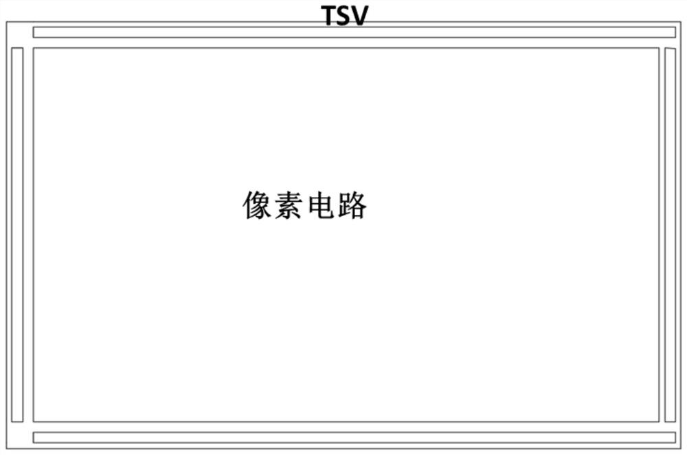
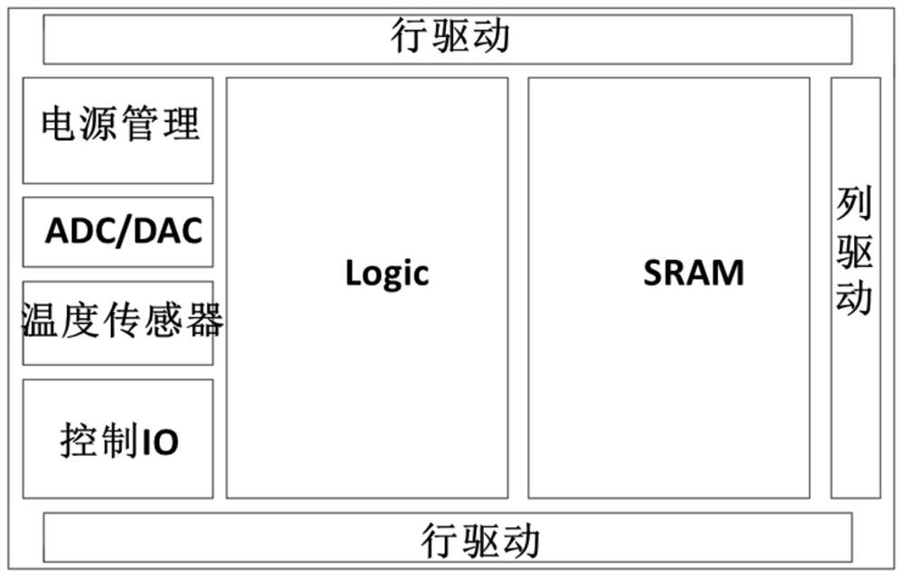
[0025] Such as Figure 2-4 As shown, the stacked micro-display driver chip architecture is composed of two independent upper pixel circuit layers and lower driver circuit layers. The pixel circuit layer and the driver circuit layer are two sheet structures, and the glue The sticky structure is together, and the edges of the facing surfaces of the pixel circuit layer and the driving circuit layer are ...


PUM


Abstract

The invention discloses a stack type micro-display driving chip architecture which comprises an upper pixel circuit layer and a lower driving circuit layer which are mutually independent, the edge of the pixel circuit layer is provided with a TSV circuit, the middle of the pixel circuit layer is provided with a pixel circuit, and the periphery of the upper surface of the driving circuit layer is provided with protruding contacts used for being electrically connected with the TSV circuit. A pixel circuit and a peripheral driving circuit are prepared separately by using a stack type framework, and then the two circuits are bonded together by using a 3D packaging technology of wafer to wafer or die to wafer, so a driving IC of 3D stacking of the pixel circuit and the peripheral driving circuit is prepared. The purposes of reducing the die pixel area, improving the yield and reducing the cost are achieved; meanwhile, the problem of poor compatibility of a traditional driving IC is solved, and the requirements of large driving current of a pixel circuit and high speed of a driving circuit can be met; and power consumption and heating are reduced.

Description

technical field [0001] The invention relates to the technical field of micro-display driving. Background technique [0002] Silicon-based MOSFET (metal-oxide-semiconductor field-effect transistor) driver ICs have been widely used in the field of microdisplays, including silicon-based organic light-emitting diodes (silicon-based OLEDs), liquid crystals on silicon (LCOS), Micro LEDs, digital light processing ( DLP), etc., have achieved ultra-high resolution with the help of high carrier mobility (~1350cm2 / Vs) of single crystal silicon. The traditional micro-display driver IC includes two parts: pixel circuit and peripheral circuit. The pixel circuit is a repeated circuit array, which is used to drive the optical structure and display images; the peripheral circuit includes row driver circuit, column driver circuit, storage circuit (SRAM), logic operation Circuit (logic), analog-to-digital / digital-to-analog conversion module (ADC / DAC), control IO circuit, power management modu...

Claims


Application Information

Patent Timeline
Patent Type & Authority Applications(China)
IPC IPC(8): G09G3/3208G09G3/32G09G3/36
CPCG09G3/32G09G3/3208G09G3/3611
Inventor 吕迅刘晓佳刘胜芳曹贺乔程陆瑞
Owner ANHUI SEMICON INTEGRATED DISPLAY TECH CO LTD
Why Eureka
Try Eureka