A 3D stacked fan-out package structure and its manufacturing method

A packaging structure, fan-out technology, which is applied in semiconductor/solid-state device manufacturing, semiconductor devices, semiconductor/solid-state device components, etc. It is difficult to reduce the volume of stacked packaging and other problems, so as to achieve the effect of reducing packaging cost, low loss and short response time

Active Publication Date: 2021-09-24
江苏长晶科技股份有限公司
View PDF6 Cites 0 Cited by
  • Summary
  • Abstract
  • Description
  • Claims
  • Application Information

AI Technical Summary

Problems solved by technology

This kind of 2.5D / 3D wafer-level packaging has limited integration, and it is difficult to carry out wafer-level testing in TSV technology. It is difficult to guarantee the yield rate of chips, and the final packaging yield is low, which in turn increases the cost of packaging.
In addition, in the case of stacked package layers, it is difficult to reduce the volume of the stacked package due to the large number of intermediate layers, and this type of package will also increase the volume of the package due to the problem of assembly accuracy.

Method used


Image

  • A 3D stacked fan-out package structure and its manufacturing method
  • A 3D stacked fan-out package structure and its manufacturing method
  • A 3D stacked fan-out package structure and its manufacturing method

Examples


Embodiment Construction

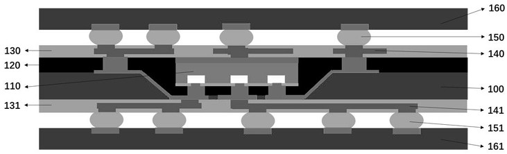
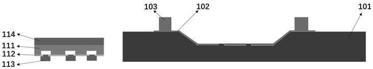
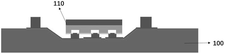
[0022] The technical means adopted by the present invention to achieve the intended invention purpose are further described below in conjunction with the drawings and preferred embodiments of the present invention. In the various figures, identical elements are indicated with similar reference numerals. For the sake of clarity, various parts in the drawings have not been drawn to scale. Additionally, some well-known parts may not be shown. For the sake of simplicity, the semiconductor structure obtained after several steps can be described in one figure.

[0023] In the following, many specific details of the present invention are described, such as device structures, materials, dimensions, processing techniques and techniques, for a clearer understanding of the present invention. However, the invention may be practiced without these specific details, as will be understood by those skilled in the art.

[0024]It should be noted that the embodiment of the present invention d...


PUM


Abstract

The invention discloses a fan-out packaging structure with 3D stacking and back-leading and a manufacturing method thereof. The fan-out packaging structure includes a carrier board (wafer), a chip, a plastic encapsulation layer, a first redistribution layer, a first dielectric layer, a second redistribution layer and a second dielectric layer. The fan-out packaging structure realizes double-sided fan-out, which can effectively reduce the packaging cost and broaden the application range of the structure; this structure mainly relies on the design of the substrate to realize the interconnection of the front and back sides of the chip, rather than based on TSV through holes, which can It effectively reduces the difficulty of the process, and the processing and production can be realized by using general-purpose equipment; in addition, the fan-out packaging structure can shorten the connection distance, which has great advantages in product performance, especially electrical performance and signal transmission, and its loss is smaller. More efficient and faster response times.

Description

technical field [0001] The present invention relates to semiconductor wafer packaging technology, more specifically, to a 3D stacked fan-out package structure and a manufacturing method thereof. Background technique [0002] With the development of semiconductor technology, semiconductor devices are becoming more and more complex, and the volume of semiconductor devices is also becoming smaller and smaller. In addition, semiconductor devices are required to have more functions and faster processing speeds. In order to support the increased functions, the semiconductor package including these components has a large number of contact pads for external electrical connection, such as for input or output, these contact pads will greatly increase the surface area of ​​the semiconductor package, and even occupy the semiconductor half of the package surface area. [0003] The traditional wafer-level packaging technology uses fan-in technology (Fan-in), which requires that the chip...

Claims


Application Information

Patent Timeline
Patent Type & Authority Patents(China)
IPC IPC(8): H01L23/498H01L23/31H01L25/04H01L21/60H01L21/50H01L21/52H01L21/56
CPCH01L21/50H01L21/52H01L21/568H01L23/3128H01L23/498H01L23/49805H01L23/49816H01L23/49838H01L24/02H01L24/03H01L25/04H01L2224/02311H01L2224/0233H01L2224/02331H01L2224/02379
Inventor 杨国江高军明
Owner 江苏长晶科技股份有限公司
Why Eureka
Try Eureka