UV-LED based on asymmetric quantum well structure and preparation method thereof

A UV-LED, asymmetric technology, applied in semiconductor devices, electrical components, circuits, etc., can solve the problems of narrow spectrum, narrow luminescence peak, single quantum well structure, etc., to achieve the effect of good performance

Active Publication Date: 2021-08-24
NANJING UNIV
View PDF0 Cites 0 Cited by
  • Summary
  • Abstract
  • Description
  • Claims
  • Application Information

AI Technical Summary

Problems solved by technology

[0002] The active layer of the traditional UV-LED structure generally adopts 3-5 periodic symmetric quantum wells. The quantum well structure of the traditional UV-LED is single and completely symmetrical, and the obtained spectrum is narrow
At present, ultraviolet LEDs have the problem of narrow luminescence peaks; due to the lack of deep ultraviolet phosphors, it is impossible to realize the wide-spectrum luminescence of ultraviolet LEDs like the combination of blue LEDs and phosphors to form white light. It is urgent to develop a wide-spectrum ultraviolet LED based on a single chip.

Method used


Image

  • UV-LED based on asymmetric quantum well structure and preparation method thereof
  • UV-LED based on asymmetric quantum well structure and preparation method thereof
  • UV-LED based on asymmetric quantum well structure and preparation method thereof

Examples


Embodiment 1

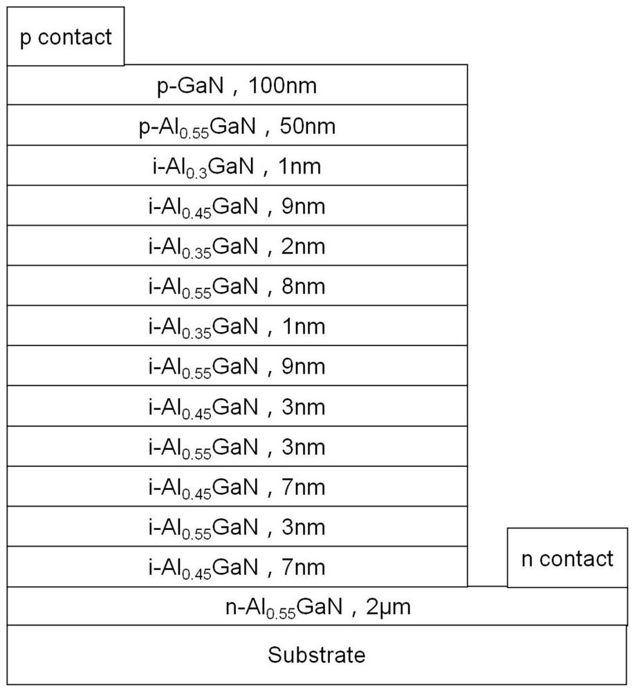
[0039] Such as figure 1 Shown, preparation is based on asymmetric quantum well structure UV-LED, and its steps include:

[0040] (1) Deposition of n-type Al on the surface of sapphire substrate by MOCVD method 0.55 Ga 0.45 N layers, such as figure 1 Shown; growing n-type Al 0.55 Ga 0.45 N layer method: trimethylgalliumtrimethylaluminum and NH 3 As Ga source, Al source and N source respectively, the carrier gas is H 2 or N 2 , the growth temperature is 1000℃, the growth thickness is 2μm, the doping source is methane, and the carrier concentration is 1*10 18 -1*10 19 cm -3 ;

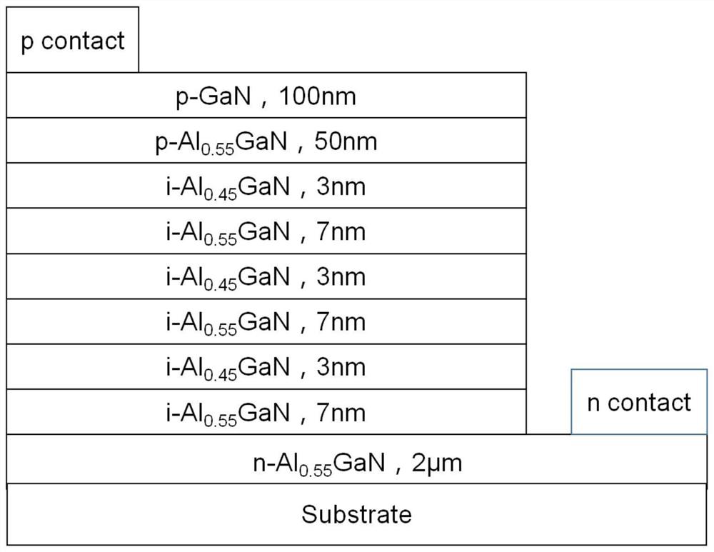
[0041] (2) MBE method in n-type Al 0.55 Ga 0.45 N-layer epitaxial Al with 2 cycles 0.45 Ga 0.55 N / Al 0.55 Ga 0.45 N quantum wells, such as figure 2 Shown; metal Ga, Al as the metal source, N plasma provides the N source, the growth temperature is 900 ° C, Al 0.45 Ga 0.55 N thickness is 3nm, Al 0.55 Ga 0.45 N thickness is 7nm;

[0042] (3) MBE method in 2 cycles of Al 0.45 Ga 0.55 N...


PUM

PropertyMeasurementUnit
Thicknessaaaaaaaaaa
Thicknessaaaaaaaaaa
Doping concentrationaaaaaaaaaa

Abstract

The invention discloses a UV-LED based on an asymmetric quantum well structure. The UV-LED structurally comprises from bottom to top: a substrate layer; an n-AlGaN layer which is grown on the substrate layer; a symmetric AlGaN quantum well layer which is grown on the n-type AlGaN layer; an asymmetric AlGaN quantum well layer which is grown on the symmetric AlGaN quantum well layer; a p-AlGaN layer which is grown on the asymmetric AlGaN quantum well layer; a p-GaN layer which is grown on the p-AlGaN layer; and a p-type electrode and an n-type electrode. The invention provides an AlGaN-based wide-spectrum ultraviolet LED (UV-LED) based on an asymmetric multi-quantum well structure, a wide luminescent spectrum is obtained through the combination of a plurality of quantum well structures with different Al components and different thicknesses, and under the bias of 6V forward voltage, the full width at half maximum of the luminescent spectrum is 17nm and is close to two times of that of a traditional UV-LED.

Description

technical field [0001] The invention relates to a UV-LED based on an asymmetric quantum well structure and a preparation method thereof. Background technique [0002] The active layer of the traditional UV-LED structure generally adopts 3-5 periodic symmetric quantum wells. The quantum well structure of the traditional UV-LED is single and completely symmetrical, and the obtained spectrum is narrow. At present, ultraviolet LEDs have the problem of narrow luminescence peaks; due to the lack of deep ultraviolet phosphors, it is impossible to realize the wide-spectrum luminescence of ultraviolet LEDs like the combination of blue LEDs and phosphors to form white light. It is urgent to develop a wide-spectrum ultraviolet LED based on a single chip. . Contents of the invention [0003] The object of the present invention is to provide a UV-LED based on an asymmetric quantum well structure, which has a wide luminescence spectrum. [0004] The object of the present invention is ...

Claims


Application Information

Patent Timeline
IPC IPC(8): H01L33/06H01L33/32H01L33/00
CPCH01L33/06H01L33/32H01L33/007
Inventor 陈敦军欧阳雨微张荣郑有炓
Owner NANJING UNIV
Why Eureka
Try Eureka