Quantum dot molecular light emitting device

A technology of molecular light-emitting and light-emitting devices, applied in phonon exciters, laser parts, lasers, etc., to achieve the effect of broadening the scope of application and improving performance

Inactive Publication Date: 2013-04-24
HUAZHONG UNIV OF SCI & TECH
View PDF0 Cites 0 Cited by
  • Summary
  • Abstract
  • Description
  • Claims
  • Application Information

AI Technical Summary

Problems solved by technology

[0009] After searching, there is no report on light-emitting devices using quantum dot molecules as the active region structure

Method used


Image

  • Quantum dot molecular light emitting device
  • Quantum dot molecular light emitting device
  • Quantum dot molecular light emitting device

Examples


Embodiment 1

[0031] Example 1. Molecular active region structure of indium arsenic quantum dots grown on a gallium arsenic substrate

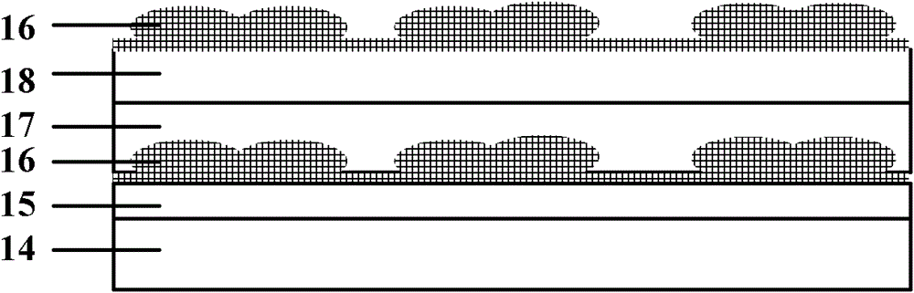
[0032] In this embodiment, the quantum dot molecular active region structure includes two layers of indium arsenic quantum dot molecules, such as figure 1 shown.

[0033] On the gallium arsenic substrate 2, epitaxial growth is sequentially grown from bottom to top using metal organic compound vapor deposition equipment:

[0034] Gallium arsenide buffer layer 3, the growth thickness is 500 nanometers, and the growth temperature is 680 degrees Celsius;

[0035] Quantum dot molecular layer 6, the quantum molecules are made of indium arsenic material, the deposition amount of indium arsenic is 1.8 atoms per layer, and the growth temperature is 511 degrees Celsius;

[0036] The stress buffer layer 7 has a thickness of 8 nanometers, and the growth temperature is the same as the growth temperature of the indium arsenic quantum dot molecules (511 degrees Celsius)...

Embodiment 2

[0040] Example 2. Light-emitting devices with indium arsenic quantum dot molecules as active region structures

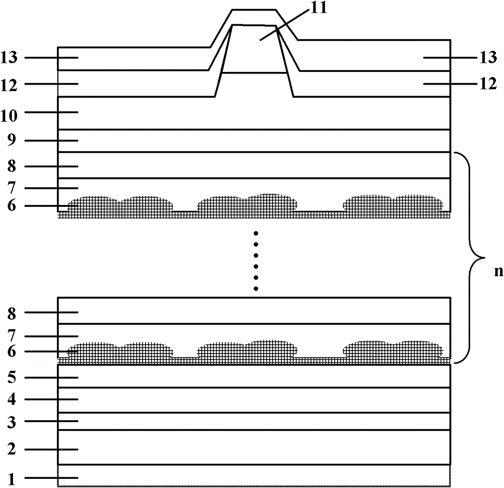
[0041] figure 2 It is a structural cross-sectional view of a light-emitting device in which the quantum dot molecules of the present invention have an active region structure, and can be applied to semiconductor lasers, semiconductor optical amplifiers, semiconductor light-emitting diodes and superluminescent light-emitting tubes.

[0042] In this embodiment, the quantum dot molecular light-emitting device includes the following structures from bottom to top: a lower gold-germanium-nickel metal electrode layer 1, a gallium-arsenic substrate 2, a gallium-arsenic buffer layer 3, an n-type aluminum-gallium-arsenic lower cladding layer 4, GaAs lower confinement waveguide layer 5, quantum dot molecular active region, GaAs upper confinement waveguide layer 9, p-type AlGaAs upper cladding layer 10, p-type GaAs ohmic contact layer 11, silicon dioxide insulating layer 12, u...


PUM

PropertyMeasurementUnit
widthaaaaaaaaaa

Abstract

The invention relates to a quantum dot molecular light emitting device, which sequentially comprises the following structures from bottom to top: a lower gold germanium nickel metal electrode layer (1), a gallium arsenic substrate (2), a gallium arsenic buffer layer (3), a n-type aluminum gallium arsenic lower cladding layer (4), a gallium arsenic lower waveguide limiting layer (5), a quantum dotmolecular active area, a gallium arsenic upper waveguide limiting layer (9), a p-type aluminum gallium arsenic upper cladding layer (10), a p-type gallium arsenic ohmic contact layer (11), a dioxide silicon insulating layer (12) and an upper titanium platinum gold metal electrode layer (13), wherein the quantum dot molecular active area comprises n quantum dot molecular layers each of which comprises quantum dot molecules (6), a stress buffer layer (7) and an isolated layer (8), and n is a natural number not less than 1. According to the invention, the laterally coupled quantum dot molecules are utilized to manufacture an active area structure and corresponding light emitting devices, thereby widening the applicable scope of quantum dot and improving the performance of low dimension semiconductor device.

Description

technical field [0001] The invention relates to the technical field of semiconductor devices, in particular to a light-emitting device with quantum dot molecules as active region structures. The light-emitting device specifically includes superluminescent light-emitting tubes, semiconductor lasers, semiconductor light-emitting diodes and semiconductor optical amplifiers. Background technique [0002] - The low-dimensional nanostructure formed by the group compounds is one of the hot topics in the research of semiconductor materials, which has great potential and broad market prospects for improving the performance of semiconductor devices. in Group elements include boron, aluminum, gallium, indium, thallium, The group elements include nitrogen, phosphorus, arsenic, antimony, and bismuth, and the compounds formed mainly include indium arsenic, indium gallium arsenic, indium phosphide, gallium arsenic, gallium phosphide, gallium arsenic antimony, indium gallium phosphid...

Claims


Application Information

Patent Timeline
Patent Type & Authority Patents(China)
IPC IPC(8): G02F1/017H01L33/30H01L31/12H01L33/04H01L33/00H01S5/343
Inventor 田芃黄黎蓉石中卫黄德修元秀华阎利杰
Owner HUAZHONG UNIV OF SCI & TECH
Why Eureka
Try Eureka