Method and element for realizing near-field display and far-field holography based on nanometer microcavity

A microcavity and nanotechnology, applied in optical components, instruments, optics, etc., can solve problems such as constrained holographic bandwidth, high precision requirements, complex microstructure, etc., to achieve the effect of avoiding holographic bandwidth, low precision requirements, and easy design

Active Publication Date: 2021-08-27
WUHAN UNIV
View PDF7 Cites 0 Cited by
  • Summary
  • Abstract
  • Description
  • Claims
  • Application Information

AI Technical Summary

Problems solved by technology

[0004] However, the microstructure of metasurface processing is relatively complex, requires high precision, and the corresponding manufacturing cost is also high.
At the same time, since the near-field spectrum is highly consistent with the spectral range that can achieve far-field holography, it leads to the problem that the near-field spectrum constrains the holographic bandwidth.

Method used


Image

  • Method and element for realizing near-field display and far-field holography based on nanometer microcavity
  • Method and element for realizing near-field display and far-field holography based on nanometer microcavity
  • Method and element for realizing near-field display and far-field holography based on nanometer microcavity

Examples


Embodiment Construction

[0034] In order to make the purpose, technical solutions and advantages of the embodiments of the present invention clearer, the technical solutions in the embodiments of the present invention will be clearly and completely described below in conjunction with the drawings in the embodiments of the present invention. Obviously, the described embodiments It is a part of embodiments of the present invention, but not all embodiments. Based on the embodiments of the present invention, all other embodiments obtained by persons of ordinary skill in the art without making creative efforts belong to the protection scope of the present invention.

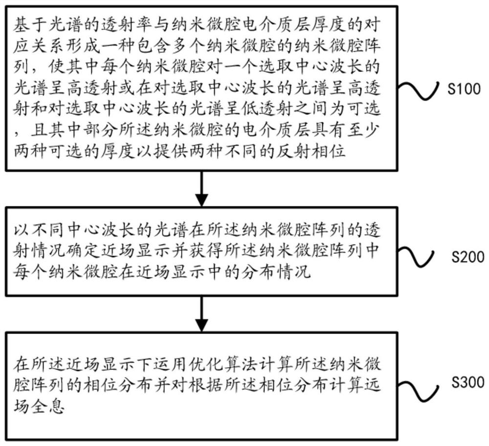
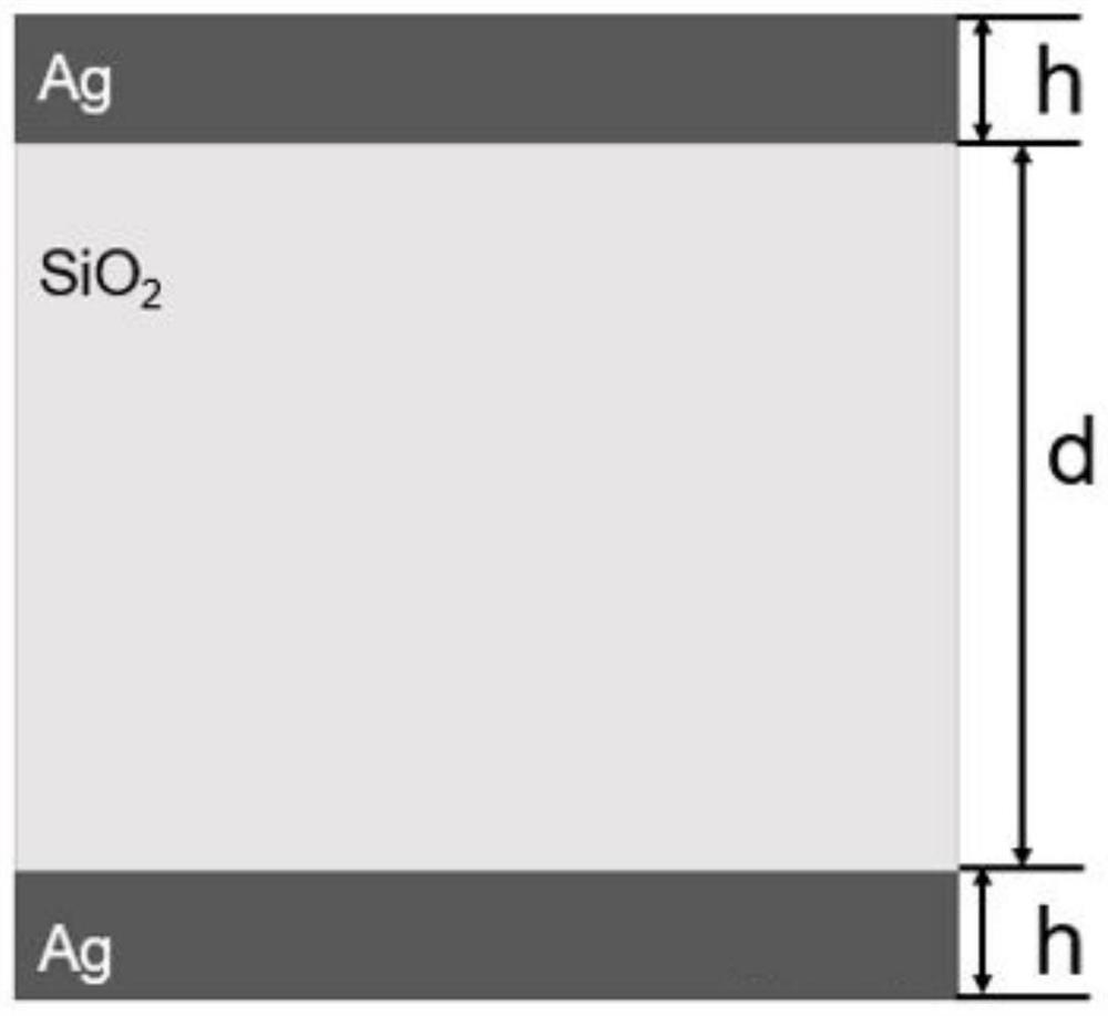
[0035] Such as figure 1As shown, the embodiment of the present invention provides a method for realizing near-field display and far-field holography based on a nano-microcavity. The nano-microcavity refers to a three-layer film structure composed of a metal layer-dielectric layer-metal layer , the method for realizing near-field display and ...


PUM


Abstract

The invention relates to a method and an element for realizing near-field display and far-field holography based on a nanometer microcavity, and the nanometer microcavity is a three-layer film structure composed of a metal layer, a dielectric layer and a metal layer. The method comprises the following steps: forming a nano micro-cavity array comprising a plurality of nano micro-cavities based on the corresponding relationship between the transmittance of a spectrum and the thickness of a nano micro-cavity dielectric layer, so that each nano micro-cavity is allowed to have high transmission for a spectrum with a selected central wavelength or be optional between the high transmission for the spectrum with the selected central wavelength and the low transmission for the spectrum with the selected central wavelength, and part of the dielectric layers of the nano microcavities have at least two optional thicknesses so as to provide two different reflection phases; determining near-field display according to the transmission conditions of the spectrums with different central wavelengths in the nano micro-cavity array; and calculating the phase distribution of the nano microcavity array by using an optimization algorithm, and calculating the far-field holography according to the phase distribution.

Description

technical field [0001] The invention relates to micro-nano optics and optical thin film technology, in particular to a method and element for realizing near-field display and far-field holography based on nano-microcavity. Background technique [0002] At present, the three-layer film structure composed of sub-wavelength metal layer-dielectric layer-metal layer can form F-P interference effect, and the nano-microcavity formed under the condition of selecting appropriate materials and thickness can show good wavelength selection. This wavelength selectivity is manifested in that when the thickness of the upper and lower metal layers is fixed, by changing the thickness of the dielectric layer, the narrow-band transmission at different central wavelengths in the visible light band can be achieved, and then the transmitted light with high saturation and different colors can be obtained. The underlying metal is set to be thicker, so as to achieve full absorption of the transmitte...

Claims


Application Information

Patent Timeline
Patent Type & Authority Applications(China)
IPC IPC(8): G03H1/04G03H1/08G03H1/16G02B27/00
CPCG03H1/0402G03H1/0841G03H1/16G02B27/0012G03H2001/085
Inventor 李仲阳王泽静代尘杰郑国兴李子乐李哲万成伟
Owner WUHAN UNIV
Why Eureka
Try Eureka