Supercharge Your Innovation With Domain-Expert AI Agents!

Analog circuit comprising high-resistance resistor and GGNMOS ESD and manufacturing method thereof

A technology for simulating circuits and manufacturing methods, applied in circuits, electrical components, electrical solid devices, etc., can solve the problems of complex process steps and high manufacturing costs

Active Publication Date: 2021-08-31
GTA SEMICON CO LTD
View PDF8 Cites 0 Cited by
  • Summary
  • Abstract
  • Description
  • Claims
  • Application Information

AI Technical Summary

Problems solved by technology

[0004] The technical problem to be solved in the present invention is in order to overcome the manufacturing process steps of the analog circuit comprising high-impedance resistor and GGNMOS ESD complex in the prior art, the defect that manufacturing cost is higher, propose a kind of analog circuit including high-impedance resistor and GGNMOS ESD and its production method

Method used


Image

  • Analog circuit comprising high-resistance resistor and GGNMOS ESD and manufacturing method thereof
  • Analog circuit comprising high-resistance resistor and GGNMOS ESD and manufacturing method thereof
  • Analog circuit comprising high-resistance resistor and GGNMOS ESD and manufacturing method thereof

Examples


Embodiment 1

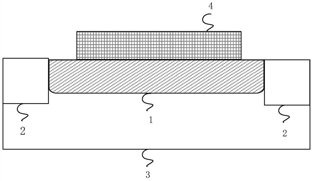
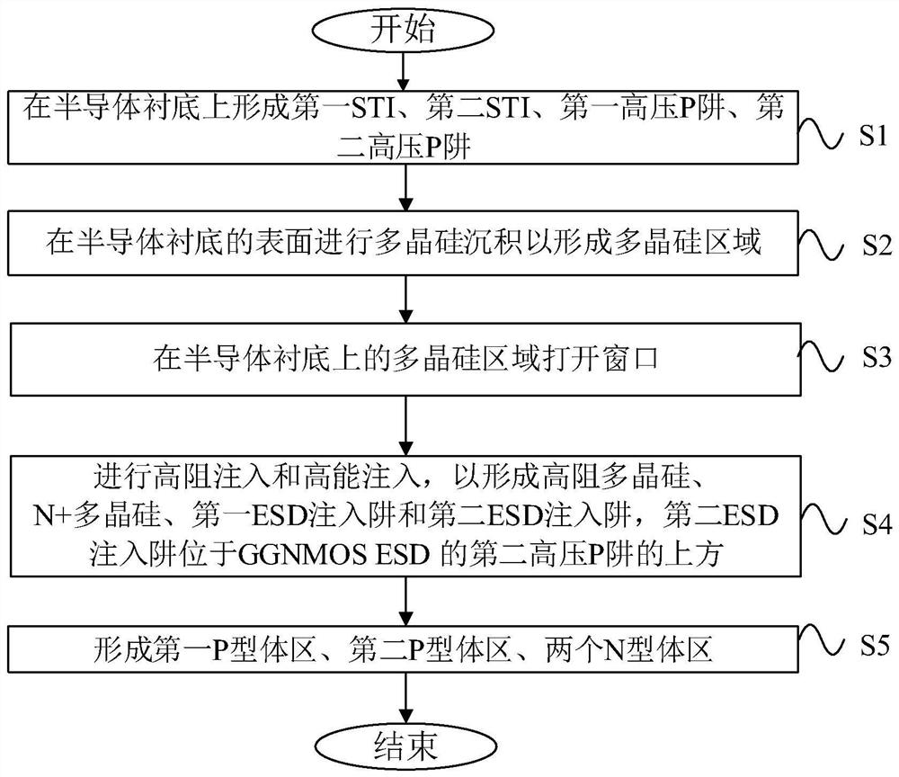
[0039] This embodiment provides a method for making an analog circuit including a high-impedance resistor and a GGNMOS ESD, such as image 3 As shown, the manufacturing method disclosed in this embodiment includes the following steps:

[0040] Step S1 , forming a first STI1 , a second STI5 , a first high voltage P well 3 , and a second high voltage P well 6 on the semiconductor substrate.

[0041] In this embodiment, when the first STI1 and the second STI5 are fabricated on the semiconductor substrate, in other words, the STI region is fabricated. Etch trenches in preset areas in the first high-voltage P well 3 and the second high-voltage P well 6 through a mask, and then fill the trenches with SiO 2 (Silicon Dioxide), using device pairs to fill SiO 2 The grooves are polished to form regions corresponding to the first STI1 and the second STI5, that is, shallow trench isolation regions.

[0042] Step S2, performing polysilicon deposition on the surface of the semiconductor s...

Embodiment 2

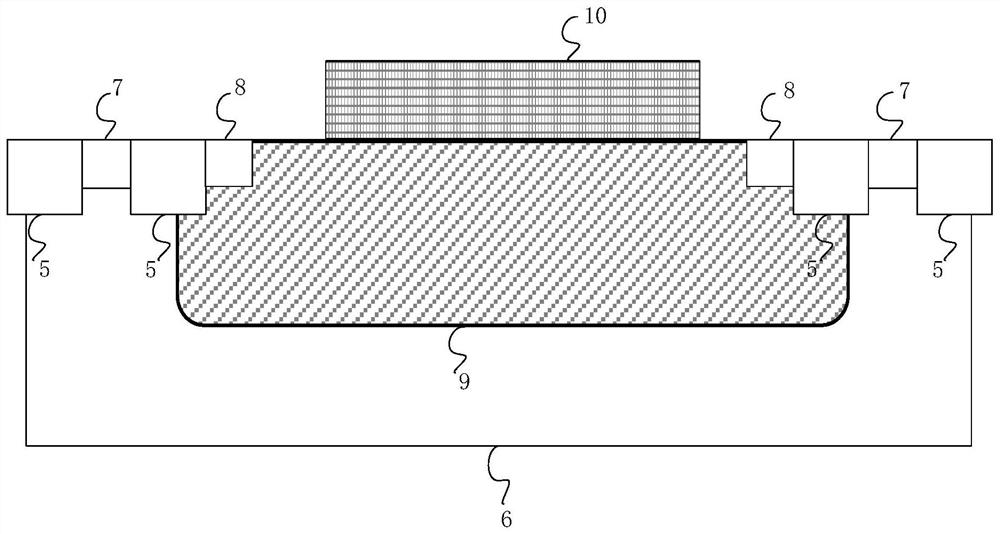
[0073] This embodiment provides an analog circuit including a high-resistance resistor and GGNMOS ESD, and the high-resistance resistor and GGNMOS ESD are manufactured using the method for manufacturing an analog circuit including a high-resistance resistor and GGNMOS ESD in Embodiment 1.

[0074] Compared with the manufacturing method of the traditional standard high-resistance resistor and GGNMOS ESD device, the analog circuit including high-resistance resistor and GGNMOS ESD provided by this embodiment uses high-resistance injection to insert high-energy ESD injection instead of a separate ESD injection well. mask, that is, the use of high-resistance injection and high-energy injection realizes the combination of two photomasks into one photomask, realizes the production of free GGNMOS ESD, solves the problem of complex analog circuit technology including high-resistance resistors and GGNMOS ESD, and saves manufacturing cost. At the same time, the efficiency of the GGNMOS E...


PUM


Abstract

The invention discloses an analog circuit comprising a high-resistance resistor and a GGNMOS ESD and a manufacturing method thereof. The method comprises steps of forming a first STI, a second STI, a first high-voltage P well and a second high-voltage P well on the semiconductor substrate, performing polycrystalline silicon deposition on the surface of the semiconductor substrate to form a polycrystalline silicon region, opening a window in the polycrystalline silicon region on the semiconductor substrate, and performing high-resistance injection and high-energy injection to form high-resistance polycrystalline silicon, N+ polycrystalline silicon, a first ESD injection well and a second ESD injection well. Two photomasks are combined into one photomask through high-resistance injection and high-energy injection, the problem that the process for manufacturing an analog circuit including a high-resistance resistor and a GGNMOS ESD is complex is solved, and the manufacturing cost is saved.

Description

technical field [0001] The invention relates to the field of semiconductor manufacturing, in particular to an analog circuit including a high-resistance resistor and a GGNMOS ESD and a manufacturing method thereof. Background technique [0002] High-resistance resistors and GGNMOS ESD (gate-grounded NMOS electrostatic discharge) are widely used in analog circuits in chip design. A cross-sectional schematic diagram of a high-resistance resistor device in an analog circuit in the prior art is shown as figure 1 As shown, the high-resistance resistor includes a first STI1 (Shallow Trench Isolation, shallow trench isolation region), a first high-voltage P-well 3 , a first P-type body region 2 and a high-resistance polysilicon 4 . The cross-sectional schematic diagram of the GGNMOSESD device in the analog circuit in the prior art is as figure 2 As shown, the GGNMOS ESD includes several second STIs 5 , a second high-voltage P well 6 , a second P-type body region 7 , two N-type b...

Claims


Application Information

Patent Timeline
Patent Type & Authority Applications(China)
IPC IPC(8): H01L21/265H01L21/336H01L27/02H01L29/66
CPCH01L21/26506H01L21/266H01L29/66568H01L27/0266
Inventor 林威朱夏
Owner GTA SEMICON CO LTD
Features
  • R&D
  • Intellectual Property
  • Life Sciences
  • Materials
  • Tech Scout
  • Unparalleled Data Quality
  • Higher Quality Content
  • 60% Fewer Hallucinations
Learn More