
Complementary metal oxide semiconductor (CMOS) digital integrated circuit total dose effect modeling method and system

A total dose effect and integrated circuit technology, applied in general control systems, control/regulation systems, simulators, etc., can solve problems such as the inability to accurately and continuously characterize the electrical characteristics of devices

Pending Publication Date: 2021-09-03
XIDIAN UNIV
View PDF0 Cites 2 Cited by
  • Summary
  • Abstract
  • Description
  • Claims
  • Application Information

AI Technical Summary

Problems solved by technology

[0014] Aiming at the problems existing in the prior art, the present invention provides a CMOS digital integrated circuit total dose effect modeling method and system, aiming at solving the problem that the existing digital integrated circuit total dose effect modeling method can only characterize the behavior of digital device ports characteristics, it is impossible to accurately and continuously characterize the electrical characteristics of devices under different conditions

Method used


Image

  • Complementary metal oxide semiconductor (CMOS) digital integrated circuit total dose effect modeling method and system
  • Complementary metal oxide semiconductor (CMOS) digital integrated circuit total dose effect modeling method and system
  • Complementary metal oxide semiconductor (CMOS) digital integrated circuit total dose effect modeling method and system

Examples


Embodiment 1

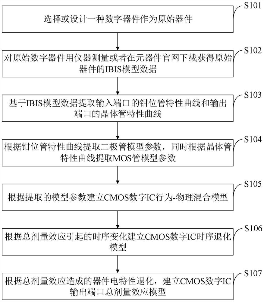
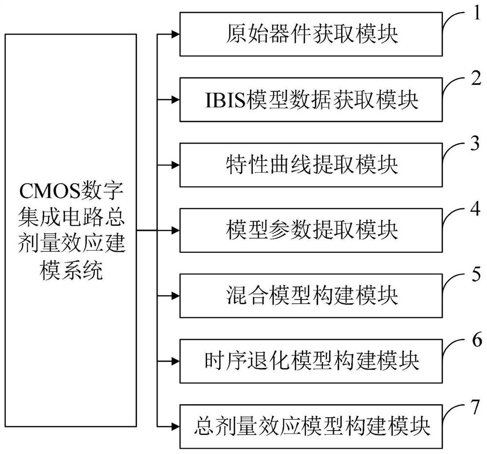
[0131] The present invention is achieved in this way, a CMOS digital integrated circuit total dose effect modeling method, said a CMOS digital integrated circuit total dose effect modeling method is obtained by measuring the original digital device with an instrument or downloading it from the official website of the component manufacturer The IBIS model data of the device; based on the IBIS model, extract the characteristic curve of the input port clamp tube and the characteristic curve of the output port transistor; extract the diode model parameters according to the clamp tube characteristic curve; extract the MOS tube model parameters according to the transistor characteristic curve; according to the extracted model parameters Establish a CMOS digital IC behavior-physical hybrid model; establish a timing degradation model based on the timing change caused by the total dose effect; finally establish a total dose effect model for the output port based on the degradation of dev...

Embodiment 2

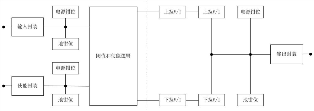
[0142] First of all, in order to model, it is necessary to select the original electronic device. The original device can be an existing device on the market, or you can design and manufacture an electronic device yourself. To obtain the IBIS model of the original electronic device, you can use the SPICE simulation method or the method of direct measurement of the real device to measure its IV data and VT data (IV data represents the current-voltage relationship, including pull-up and pull-down I / V data Pullup, Pulldown and power supply And GND clamp data Power_Clamp, Gnd_Clamp; VT data represents the voltage-time relationship, including VT data of rising waveform and VT data of falling waveform, such as image 3 shown), etc., enter the data into the IBIS file, and complete the creation of the model (for the devices purchased on the market, you can also directly obtain the IBIS model of the original device from the manufacturer).

[0143] When extracting the characteristic cur...


PUM


Abstract

The invention belongs to the technical field of digital device irradiation effect model modeling, and discloses a CMOS digital integrated circuit total dose effect modeling method and system, and the method comprises the steps: selecting or designing an original device; obtaining IBIS model data of the original device; extracting a clamping tube characteristic curve of the input port and a transistor characteristic curve of the output port; extracting diode model parameters according to the clamping tube characteristic curve, and extracting MOS tube model parameters according to the transistor characteristic curve; establishing a CMOS digital IC behavior-physical hybrid model according to the model parameters, and establishing a CMOS digital IC time sequence degradation model; and establishing a total dose effect model of the output port of the CMOS digital IC according to the electrical characteristic degradation of the device caused by the total dose effect. The model established by the invention not only can reflect the logic function of the CMOS digital device, but also provides model support for system simulation under the irradiation condition.

Description

technical field [0001] The invention belongs to the technical field of modeling of radiation effect models of digital devices, and in particular relates to a method and system for modeling total dose effects of CMOS digital integrated circuits. Background technique [0002] At present, with the rapid development of semiconductor technology, various analog and digital integrated circuits are widely used in the fields of aerospace, nuclear industry and particle physics. They are in the radiation environment of various electromagnetic and high-energy particles, and the total dose of radiation , single-event radiation and transient effects and other radiation effects, its working reliability and life cycle have been severely tested. Among them, the total dose radiation effect has received extensive attention and research. [0003] In recent years, with the development of computer simulation technology, electronic system radiation effect simulation provides strong support for sy...

Claims


Application Information

Patent Timeline
Patent Type & Authority Applications(China)
IPC IPC(8): G05B17/02
CPCG05B17/02
Inventor 刘锦辉梁博曹烨政孟菲刘刚万波
Owner XIDIAN UNIV
Learn More