
Dielectric film system design method, film coating method and cover plate

A design method and film system design technology, applied in sputtering coating, vacuum evaporation coating, ion implantation coating and other directions, can solve the problems of film cracking and strength reduction

Active Publication Date: 2021-09-10
LENS TECH CHANGSHA
View PDF5 Cites 0 Cited by
  • Summary
  • Abstract
  • Description
  • Claims
  • Application Information

AI Technical Summary

Problems solved by technology

[0005] One of the purposes of the present invention is to provide a dielectric film system design method, which alleviates the problems of film cracking and strength reduction caused by the existing coating technology in pursuit of cool effects

Method used


Image

  • Dielectric film system design method, film coating method and cover plate
  • Dielectric film system design method, film coating method and cover plate
  • Dielectric film system design method, film coating method and cover plate

Examples


Embodiment 1

[0069] Embodiment 1 (reflective purple)

[0070] 1. Design of reflective purple dielectric film system:

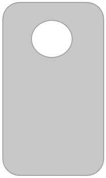
[0071] 1. Customers supply reflective purple board such as figure 1 shown.

[0072] According to the color plate analysis, this is a single color, that is, a pure color. It is found that it has no metallic texture, so it is concluded that its film system should be a dielectric film. The Lab value data obtained from the test is as follows and the target curve of the color plate is as follows figure 2 :

[0073] swatches R (reflection) T (through) L 45.93 93.69 a 25.29 -9 b -12.5 4.58 Chromaticity coordinates R (reflection) T (through) L 15.22 84.56 x 0.354 0.329 y 0.27 0.348

[0074] Import the color palette target into TFC software, and select the film material Nb 2 o 5 (Niobium pentoxide), SiO 2 (Silicon dioxide) is optimized, the optimized curve is completely consistent with the color plate target, and...

Embodiment 2

[0112] Example 2 (reflective gold)

[0113] 1. Design of reflective gold dielectric film system:

[0114] 1. Reflective gold plate for customers Figure 6 shown.

[0115] According to the color plate analysis, this is a single color, that is, a pure color. It is found that it has no metallic texture, so it is concluded that its film system should be a dielectric film. The Lab value data obtained from the test is as follows and the target curve of the color plate is as follows Figure 7 :

[0116] swatches R (reflection) T (through) L 69.75 81.55 a 15.39 -12.8 b 14.02 -9.3 Chromaticity coordinates R (reflection) T (through) L 40.39 59.46 x 0.394 0.295 y 0.348 0.324

[0117] Import the color palette target into TFC software, and select the film material Nb 2 o 5 (Niobium pentoxide), SiO 2 (Silicon dioxide) is optimized, the optimized curve is completely consistent with the color plate target, and the obtained f...


PUM

PropertyMeasurementUnit
refractive indexaaaaaaaaaa

Abstract

The invention provides a dielectric film system design method, a coating method and a cover plate, and relates to the technical field of coating, and the dielectric film system design method comprises the following steps: (a) testing a target dielectric film color plate by using a color measuring device to obtain a Lab value and a target curve of the target dielectric film color plate; (b) importing the target curve into film system design software, and selecting a film layer material for design, wherein a design curve is made to be consistent with the target curve, a film system structure is obtained, and the design curve corresponds to the Lab value and a chromaticity coordinate Lxy value; and (c) when the film thickness of the film system is greater than 500nm, re-inputting the chromaticity coordinate Lxy value obtained in the step (b) into film system design software, inputting a film thickness range and a film layer material at the same time to carry out optimization design, screening out an optimization design curve meeting requirements, obtaining an optimized film system structure, and debugging a coating film by using the designed film system structure. According to the invention, the problems of film cracking and strength reduction caused by too thick film layer of the color dielectric film in the existing film coating technology are relieved.

Description

technical field [0001] The invention relates to the field of coating technology, in particular to a dielectric film system design method, a coating method, and a cover plate. Background technique [0002] With the advent of the 5G era, smart phones, smart watches and other electronic products are widely popularized. Consumers' requirements for electronic products are not only limited to performance and lifespan, but also have higher and higher requirements for visual effects and appearance. At present, the cool-looking mobile phone back cover has become one of the design directions pursued by most consumer electronics manufacturers for mid-to-high-end models. Generally, the thicker the film thickness, the cooler the color, so when developing mobile phone covers, they often blindly pursue High film thickness to achieve cool effect. However, there are several major disadvantages of high film thickness: first, the film thickness is too thick, the film forming time is long, the...

Claims


Application Information

Patent Timeline
Patent Type & Authority Applications(China)
IPC IPC(8): G02B27/00G02B1/10C23C14/35C23C14/08C23C14/10
CPCG02B27/0012G02B1/10C23C14/35C23C14/083C23C14/10
Inventor 田兴波贾正宝龙海红朱斌陈小群
Owner LENS TECH CHANGSHA
Learn More