Semiconductor device and preparation method thereof

A technology of semiconductors and devices, applied in the field of semiconductor devices and their preparation, can solve the problems that the performance requirements of large-scale interconnection structures cannot be balanced with the performance requirements of small-scale interconnection structures

Pending Publication Date: 2021-09-10
INST OF MICROELECTRONICS CHINESE ACAD OF SCI
View PDF4 Cites 1 Cited by
  • Summary
  • Abstract
  • Description
  • Claims
  • Application Information

AI Technical Summary

Problems solved by technology

[0003] The embodiment of the present application provides a semiconductor device and its preparation method, which solves the technical problem that the performance requirements of the large-size interconnection structure and the performance requirements of the small-size int

Method used


Image

  • Semiconductor device and preparation method thereof
  • Semiconductor device and preparation method thereof
  • Semiconductor device and preparation method thereof

Examples


Embodiment 1

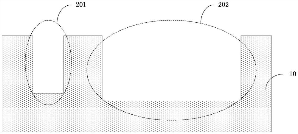
[0032] Such as figure 1 As shown, a method for preparing a semiconductor device is provided, comprising: providing a dielectric layer 10, forming a first groove 201 and a second groove 202 in the dielectric layer 10, the line width of the first groove 201 is smaller than that of the second groove The line width is 202; the first metal layer 401 is formed in the first groove 201; the second metal layer 402 is formed in the second groove 202.

[0033] S10: Provide a dielectric layer 10, and form a first groove 201 and a second groove 202 in the dielectric layer 10, the line width of the first groove 201 is smaller than the line width of the second groove 202, such as figure 2 shown.

[0034] In one embodiment, the first groove 201 penetrates the dielectric layer 10 , and the second groove 202 penetrates the dielectric layer 10 .

[0035] In one embodiment, the dielectric layer 10 includes silicon dioxide, other low dielectric constant materials, and the like.

[0036] In one...

Embodiment 2

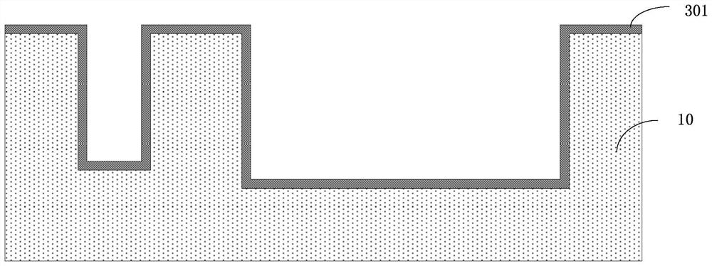
[0069] Such as Figure 7 As shown, a semiconductor device is provided, comprising: a dielectric layer 10; a first groove 201 located in the dielectric layer 10; a second groove 202 located in the dielectric layer 10, and the line width of the first groove 201 is smaller than that of the second groove. The line width of the groove 202 ; the first metal layer 401 is located in the first groove 201 ; the second metal layer 402 is located in the second groove 202 .

[0070] In one embodiment, the line width of the first groove 201 is smaller than the preset width, and the line width of the second groove 202 is larger than the preset width.

[0071] In one embodiment, the predetermined width is between 20nm˜40nm, for example, the predetermined width may be 20nm, 25nm, 30nm, 35nm, 40nm.

[0072] In one embodiment, the line width of the first groove 201 is less than 30nm, for example, the line width of the first groove 201 can be 7nm, 10nm, 15nm, 20nm, 28nm, the line width of the se...


PUM

PropertyMeasurementUnit
Widthaaaaaaaaaa
Thicknessaaaaaaaaaa

Abstract

The invention discloses a semiconductor device and a preparation method thereof. The semiconductor device comprises a dielectric layer; a first groove located in the dielectric layer; a second groove located in the dielectric layer, wherein the line width of the first groove is smaller than the preset width, and the line width of the second groove is larger than the preset width; a first metal layer located in the first groove and at the bottom and the side wall of the second groove; and a second metal layer positioned in the second groove. The technical effect that the performance requirement of a large-size interconnection structure and the performance requirement of a small-size interconnection structure are met is achieved.

Description

technical field [0001] The invention relates to the field of semiconductors, in particular to a semiconductor device and a preparation method thereof. Background technique [0002] An integrated circuit includes many interconnected structures, generally, a copper interconnection structure is used, but the inventors of the present application have found that the above-mentioned technology has at least the following technical problems: as the device size continues to shrink, the resistance of the copper interconnection structure increases sharply, and the electromigration is reliable. The problem of reliability is exacerbated, and the traditional copper interconnection technology is difficult to meet the requirements of device performance. Contents of the invention [0003] The embodiment of the present application provides a semiconductor device and its preparation method, which solves the technical problem that the performance requirements of the large-size interconnection...

Claims


Application Information

Patent Timeline
IPC IPC(8): H01L23/528H01L23/532H01L21/768
CPCH01L23/5283H01L23/53228H01L23/53242H01L23/53209H01L21/76802H01L21/76877H01L21/76847
Inventor 孙祥烈许静罗军赵超
Owner INST OF MICROELECTRONICS CHINESE ACAD OF SCI
Why Eureka
Try Eureka