Micro light-emitting diode display and manufacturing method thereof

A technology of micro-light-emitting diodes and displays, which is applied in the direction of instruments, electric solid-state devices, semiconductor devices, etc., and can solve problems such as complicated manufacturing steps, poor contact between micro-light-emitting diode chips and display backplanes, and unsuitability for rapid production of products

Pending Publication Date: 2021-09-10
CHONGQING KONKA PHOTOELECTRIC TECH RES INST CO LTD
View PDF0 Cites 1 Cited by
  • Summary
  • Abstract
  • Description
  • Claims
  • Application Information

AI Technical Summary

Problems solved by technology

However, in the prior art, after mass transfer, the micro-LED chips are only placed on the display backplane, and the position of the micro-LED chips on the display backplane is easily shifted due to external vibrations and other reasons. , resulting in poor bonding effect, poor contact between the micro-LED chip and the display backplane, which will affect the display effect of the display; and it needs to prevent external interference when producing the micro-LED display, so its The production steps are more complicated and not suitable for rapid production of products

Method used


Image

  • Micro light-emitting diode display and manufacturing method thereof
  • Micro light-emitting diode display and manufacturing method thereof
  • Micro light-emitting diode display and manufacturing method thereof

Examples


Embodiment 1

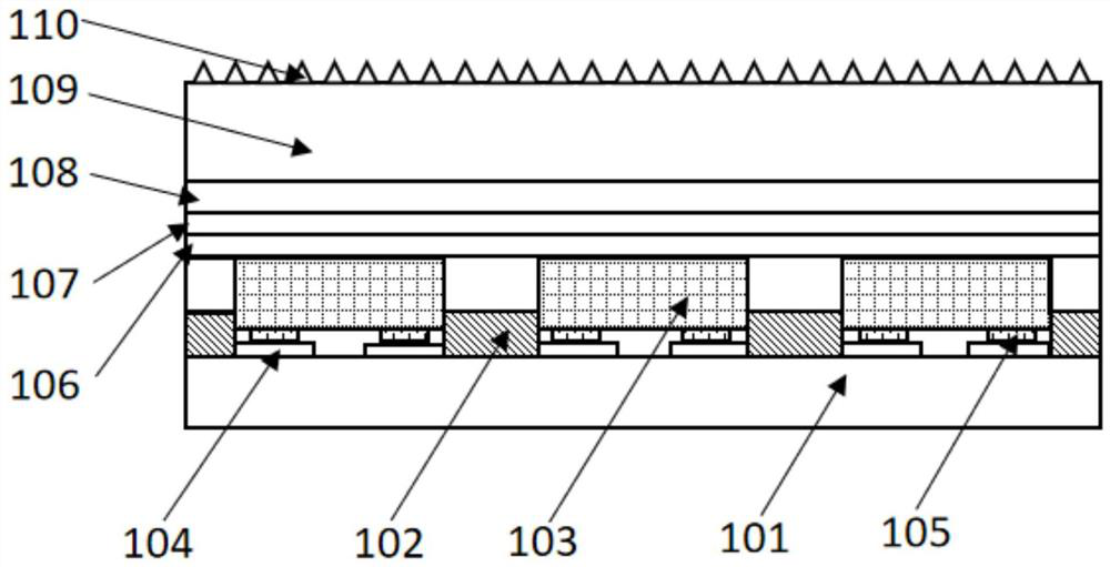
[0048] A micro light-emitting diode display of the present invention is described in detail below with an embodiment of a flip-chip display, please refer to figure 1 , which includes:

[0049]Display backplane 101, said display backplane 101 is a thin film transistor (TFT, Thin Film Transistor) backplane, said display backplane 101 is provided with three or more mutually separated limiting components, wherein the limiting component is preferably A light-shielding photoresist 102 with a light-shielding function, the light-shielding photoresist 102 includes: a white photoresist or a black photoresist; every two adjacent limiting components form an installation position for limiting the diode chip, The mounting position is matched with the side wall of the diode chip 103, and the light-shielding photoresist 102 can be connected with both sides of the metal pad assembly 104, and can also be left with a certain amount of space on both sides of the metal pad assembly 104. gap, and ...

Embodiment 2

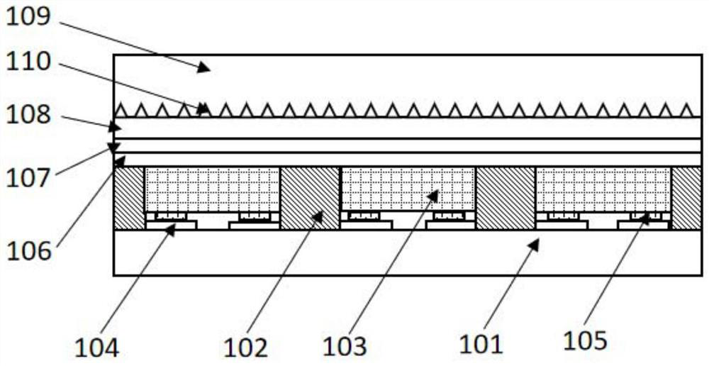
[0051] A micro light-emitting diode display of the present invention is described in detail below with another embodiment of a flip-chip display, please refer to figure 2 , which includes:

[0052] Display backplane 101, said display backplane 101 is a thin film transistor backplane, said display backplane 101 is provided with more than three mutually separated limiting components, wherein the limiting component is preferably a light-shielding photoresist with a light-shielding function 102, the light-shielding photoresist 102 includes: a white photoresist or a black photoresist; every two adjacent limiting components form an installation position for limiting the diode chip 103, and the installation position is consistent with the Cooperate with the side wall of the above-mentioned diode chip 103, the light-shielding photoresist 102 can be connected with both sides of the metal pad assembly 104, and can also leave a certain appropriate gap with the two sides of the metal pad...

Embodiment 3

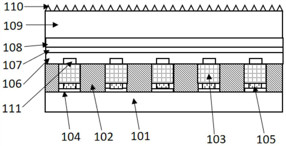
[0054] A kind of micro light-emitting diode display of the present invention is specifically described below with the embodiment of a vertical structure chip display, please refer to image 3 , which includes:

[0055] Display backplane 101, said display backplane 101 is a thin film transistor backplane, said display backplane 101 is provided with more than three mutually separated limiting components, wherein the limiting component is preferably a light-shielding photoresist with a light-shielding function 102, the light-shielding photoresist 102 includes: a white photoresist or a black photoresist; every two adjacent limiting components form an installation position for limiting the diode chip 103, and the installation position is consistent with the Cooperate with the side wall of the above-mentioned diode chip 103, the light-shielding photoresist 102 can be connected with both sides of the metal pad assembly 104, and can also leave a certain appropriate gap with the two si...


PUM


Abstract

The invention relates to the technical field of light-emitting diodes, in particular to a micro light-emitting diode display and a manufacturing method thereof. The micro light-emitting diode display comprises a display backboard, the display backboard is provided with more than three mutually-separated limiting assemblies, every two adjacent limiting assemblies form an installation position used for limiting a diode chip, the installation position is matched with the side wall of the diode chip, the bottom of each installation position is provided with a group of metal bonding pad assemblies, the metal bonding pad assemblies are fixedly arranged on the display backboard, metal contacts are bonded on the metal bonding pad assemblies and are connected with the lower end of the diode chip, the diode chip is are mounted in the instalaltion positions, and a packaging structure and a surface micro-processing layer are covered above all the diode chips and the limiting assemblies. The display is provided with the limiting assembly, so that the position of the micro light-emitting diode chip on the display backboard can be effectively limited, and the bonding effect is effectively improved; and the manufacturing steps are simplified, so that mass production of products is easy to realize.

Description

technical field [0001] The invention relates to the technical field of light emitting diodes, in particular to a micro light emitting diode display and a manufacturing method of the micro light emitting diode display. Background technique [0002] Micro LED (Mi cro LED), that is, light-emitting diode miniaturization and matrix technology, has good stability, life, and advantages in operating temperature, and also inherits LED low power consumption, color saturation, and response speed. Fast, strong contrast and other advantages, it has great application prospects. [0003] The display screen made of micro light emitting diodes is the mainstream development direction of display equipment in the future; in the manufacturing process of the existing micro light emitting diode displays, the micro light emitting diode chips need to be generated on the growth substrate first; Transfer to the display backplane and bond for fixation. However, in the prior art, after mass transfer, ...

Claims


Application Information

Patent Timeline
Patent Type & Authority Applications(China)
IPC IPC(8): H01L27/15H01L33/48G09F9/33
CPCH01L27/156H01L33/483G09F9/33H01L2933/0033H01L2933/0066
Inventor 安金鑫林子平李刘中肖守均张雪
Owner CHONGQING KONKA PHOTOELECTRIC TECH RES INST CO LTD
Why Eureka
Try Eureka