Nanostructure substrate
A substrate and structure technology, applied in the field of nanostructured substrates, can solve the problems of uneven local heating field and the like
- Summary
- Abstract
- Description
- Claims
- Application Information
AI Technical Summary
Problems solved by technology
Method used
Image
Examples
Embodiment 1
[0105]
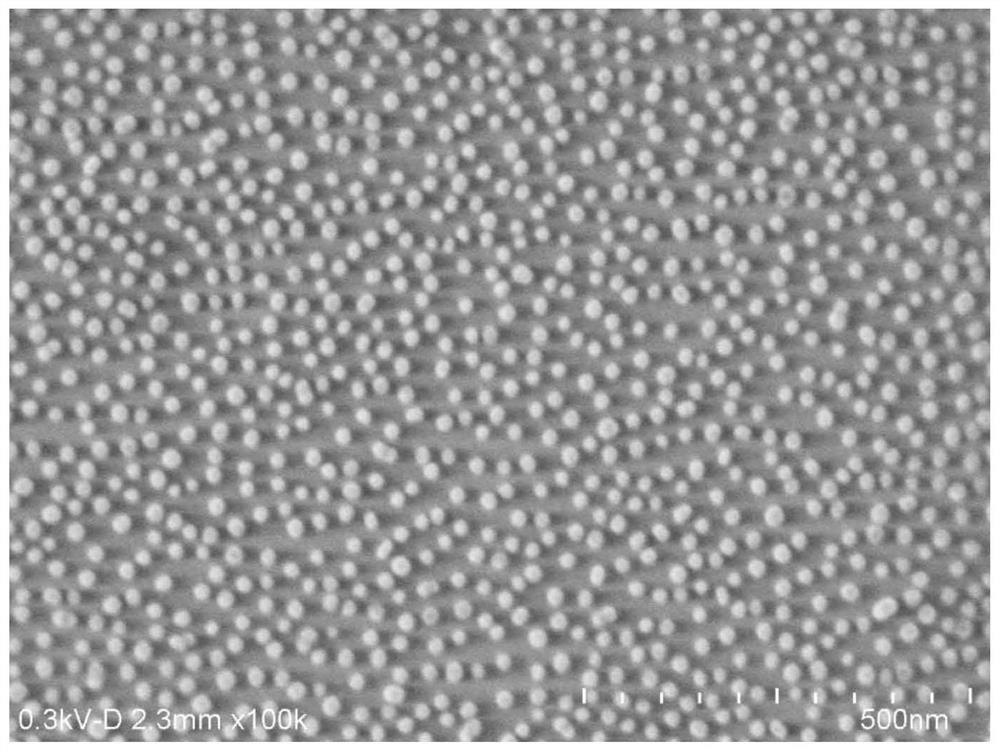
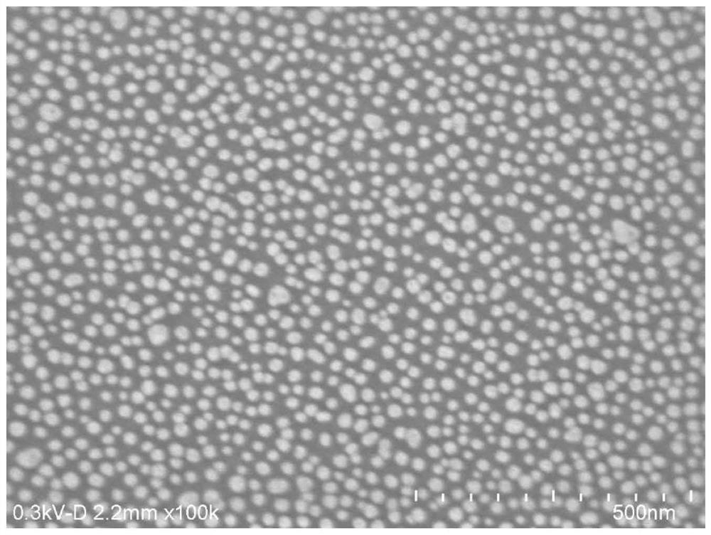
[0106] Next, this transparent substrate was immersed in a 65° C. electroless gold plating solution (improved bath of PRECIOUSFAB ACG3000WX manufactured by Electroplating Engineers of Japan Co., Ltd.) for 10 seconds as one cycle. Repeat this step for 3 cycles to form a gold coating layer. That is, gold crystal grains are deposited on the fixed gold microparticle group. which is displayed on image 3 .
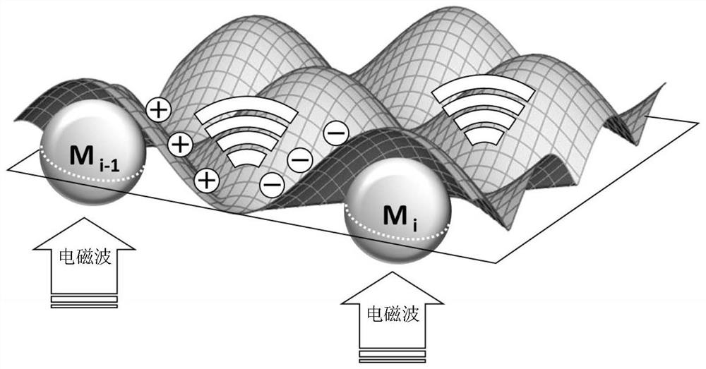
[0107] From image 3 It can be seen that in the gold coating layer, the diameter of most of the gold fine particle groups increases to become a mushroom shape, and when viewed from above, it grows into a hemispherical shape. Such as figure 1 As shown, the geometric surface area of the surface side of the composite particle group is larger than that of the back side. The average particle diameter of the gold coating layer was measured from the image of the scanning electron microscope, and the average particle diameter of the gold coating layer was in the range ...
Embodiment 2
[0112]
[0113] The electroless gold plating step was repeated for 3 more cycles, and as a result, the color of the nanostructured substrate changed from blue-purple to dark purple. An image of the heat-treated nanostructured substrate viewed from the surface side is shown in Figure 4 . Figure 4 The origin of the sea-island structure corresponding to Embodiment 2 can still be seen in the figure.
[0114] again, Figure 4 In , it is observed that a large number of gold coating layers are connected to grow into L-shaped blocks. In addition, traces of multiple gold coating layers can be observed in this L-shaped block. From this, it can be seen that the height of the gold coating layer is different in the L-shaped block. Also, the geometric surface area on the front side of the composite particle group is larger than the geometric surface area on the back side.
[0115] The absorption spectrum distribution of gold was observed in the same manner as in Example 1. This ab...
Embodiment 3
[0118] The electroless gold plating step was repeated for 3 cycles to produce a gold coating layer. Such as Figure 5 As shown, it is observed that the black part of the sea begins to disappear. It can be said to be the final stage of island structure. Because the composite particle population remains spherical, the geometric surface area on the surface side of the composite particle population is greater than the geometric surface area on the rear side. The color of the nanostructured substrate changed from blue-purple to gold. Figure 6 The uppermost curve in is the plasmonic sub-curve of Example 3.
[0119] As can be clearly seen from the results of the above examples and conventional examples, if the nanostructured substrate formed by the coating layer of the present invention is used, it can be seen that the absorbance is increased compared with the comparative example. That is, it was found that when electromagnetic waves are incident on the nanostructure substrate o...
PUM
| Property | Measurement | Unit |
|---|---|---|
| diameter | aaaaa | aaaaa |
| particle diameter | aaaaa | aaaaa |
| particle size | aaaaa | aaaaa |
Abstract
Description
Claims
Application Information


