Supercharge Your Innovation With Domain-Expert AI Agents!

Preparation method of flash memory

A technology of flash memory and storage area, which is applied in the direction of electrical components, electric solid-state devices, circuits, etc., and can solve the problems of shortening the width of floating gate and control gate, affecting the electrical performance of flash memory, affecting the erasing and reading and writing capabilities of flash memory, etc.

Pending Publication Date: 2021-09-14
SHANGHAI HUAHONG GRACE SEMICON MFG CORP
View PDF0 Cites 1 Cited by
  • Summary
  • Abstract
  • Description
  • Claims
  • Application Information

AI Technical Summary

Problems solved by technology

Flash memory has a floating gate and a control gate. The width of the floating gate and the control gate affects the erasing and reading and writing capabilities of the flash memory, and the width of the floating gate and the control gate may be affected by the preparation process, resulting in shortening of the width of the floating gate and the control gate. , ultimately affecting the electrical performance of the flash memory

Method used


Image

  • Preparation method of flash memory
  • Preparation method of flash memory
  • Preparation method of flash memory

Examples


preparation example Construction

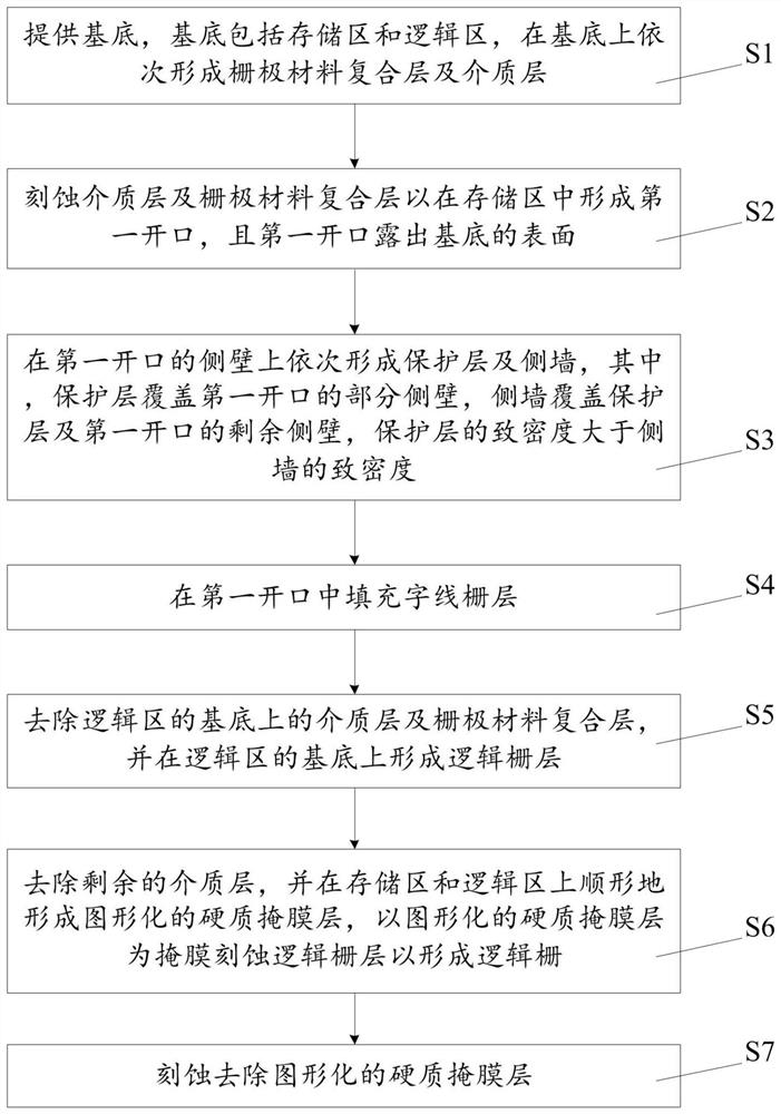
[0034] figure 1 It is a flow chart of the preparation method of the flash memory provided in this embodiment. This embodiment provides a method for preparing a flash memory, so as to improve the electrical performance of the flash memory. Please refer to figure 1 , the preparation method of flash memory comprises:

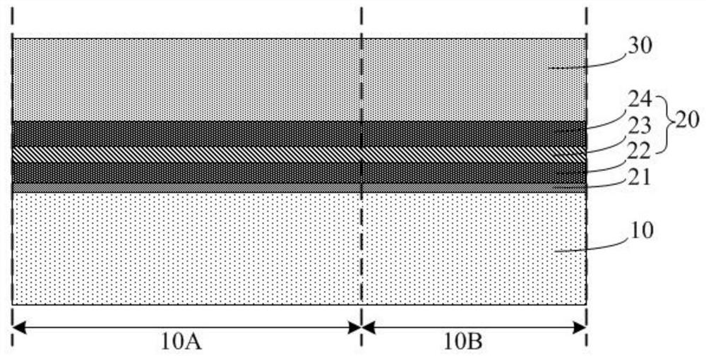
[0035] Step S1: providing a substrate, the substrate includes a storage area and a logic area, and sequentially forming a gate material composite layer and a dielectric layer on the substrate;

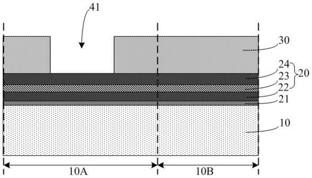
[0036] Step S2: etching the dielectric layer and the gate material composite layer to form a first opening in the storage area, and the first opening exposes the surface of the substrate;

[0037] Step S3: sequentially forming a protective layer and a sidewall on the sidewall of the first opening, wherein the protective layer covers part of the sidewall of the first opening, the sidewall covers the protective layer and the remaining sidewall of the first opening, and the...


PUM


Abstract

The invention provides a preparation method of a flash memory, which comprises the following steps of: providing a substrate which comprises a storage area and a logic area, and sequentially forming a grid material composite layer and a dielectric layer on the substrate; etching the dielectric layer and the gate material composite layer to form a first opening in the storage region; sequentially forming a protective layer and a side wall on the side wall of the first opening; filling a word line gate layer in the first opening; removing the dielectric layer and the gate material composite layer on the substrate of the logic region, and forming a logic gate layer on the substrate of the logic region; removing the residual dielectric layer, forming a patterned hard mask layer on the storage region and the logic region in a conformal manner, and etching the logic gate layer by taking the patterned hard mask layer as a mask to form a logic gate; and etching to remove the patterned hard mask layer. The electrical performance of the flash memory is improved.

Description

technical field [0001] The invention relates to the technical field of semiconductors, in particular to a method for preparing a flash memory. Background technique [0002] Flash memory has become a research hotspot in non-volatile memory due to its convenience, high storage density, and good reliability, and flash memory is widely used in mobile and communication devices such as mobile phones, notebooks, handheld computers, and U disks. As a non-volatile memory, flash memory works by changing the critical voltage of the transistor or memory cell to control the switch of the gate channel to achieve the purpose of storing data, so that the data stored in the memory will not be interrupted by the power supply And disappeared, and flash memory is a special structure of electrically erasable and programmable read-only memory. Today, flash memory has occupied most of the market share of non-volatile semiconductor memory, becoming the fastest growing non-volatile semiconductor me...

Claims


Application Information

Patent Timeline
Patent Type & Authority Applications(China)
IPC IPC(8): H01L27/11517H01L27/11521H10B41/00H10B41/30
CPCH10B41/00H10B41/30
Inventor 沈思杰周海洋
Owner SHANGHAI HUAHONG GRACE SEMICON MFG CORP
Features
  • R&D
  • Intellectual Property
  • Life Sciences
  • Materials
  • Tech Scout
  • Unparalleled Data Quality
  • Higher Quality Content
  • 60% Fewer Hallucinations
Learn More