Pulsed laser deposition device and method

A technology of pulsed laser deposition and laser device, which is applied in metal material coating process, vacuum evaporation plating, coating, etc., can solve the problem of inability to realize large-scale, large-area, high-quality thin film preparation, inability to purchase in large quantities, inability to Purchasing equipment and other issues to achieve high deposition temperature consistency, improve stability, and reduce energy loss

Pending Publication Date: 2021-09-28
SONGSHAN LAKE MATERIALS LAB
View PDF4 Cites 7 Cited by
  • Summary
  • Abstract
  • Description
  • Claims
  • Application Information

AI Technical Summary

Problems solved by technology

[0004] It can be seen that practical superconducting thin films have irreplaceable strategic and economic needs, but there is still a gap between my country and the international advanced level. For example, the preparation of high-quality large-area YBCO double-sided thin films needs to overcome a series of application foundations and key technical problems.
If the corresponding equipment and superconducting film purchased from abroad are used, on the one hand, the price is high, and it is impossible to purchase in large quantities; film preparation

Method used


Image

  • Pulsed laser deposition device and method
  • Pulsed laser deposition device and method
  • Pulsed laser deposition device and method

Examples


Embodiment Construction

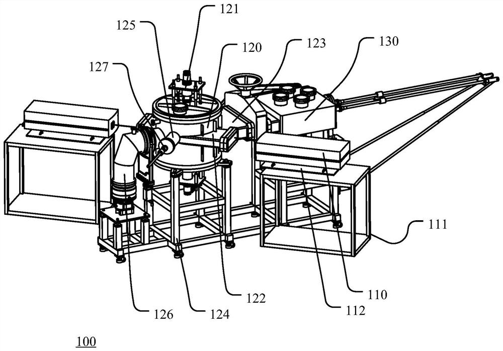
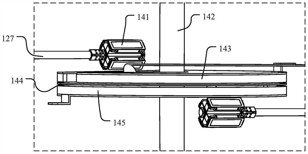
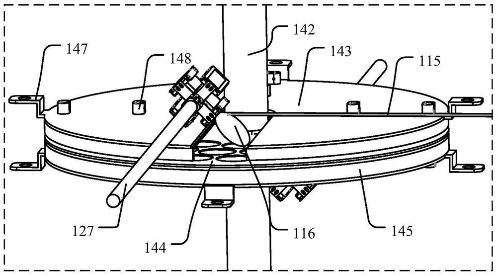
[0038] Hereinafter, the present invention will be described in more detail with reference to the accompanying drawings. In the various figures, identical elements are indicated with similar reference numerals. For the sake of clarity, various parts in the drawings have not been drawn to scale. Also, some well-known parts may not be shown. For the sake of simplicity, the semiconductor structure obtained after several steps can be described in one figure.

[0039] It should be understood that when describing the structure of a device, when a layer or a region is referred to as being "on" or "over" another layer or another region, it may mean being directly on another layer or another region, or Other layers or regions are also included between it and another layer or another region. Also, if the device is turned over, the layer, one region, will be "below" or "beneath" the other layer, or region.

[0040] If it is to describe the situation directly on another layer or anothe...


PUM


Abstract

The invention discloses a pulsed laser deposition device. The pulsed laser deposition device comprises a reaction cavity, a plurality of target machines, and a plurality of laser devices, wherein the reaction cavity is internally provided with a supporting column used for fixing a substrate table, a first heating element located above the substrate table and a second heating element located below the substrate table, target materials are fixed at the second ends of the target machines, the target materials are located above and/or below the substrate table in the reaction cavity, included angles are formed between the surfaces of the target materials and the surface of the substrate table, the plurality of laser devices respectively generate laser beams, the first heating element and the second heating element are both provided with notches, and the laser beams linearly reach the surfaces of the target materials in the direction parallel to the surface of the substrate table, and plasma formed by irradiating the surfaces of the target materials through the laser beams reaches the surface of the substrate table through the notches in the first heating element and the second heating element. According to the pulsed laser deposition device, a double-sided skew symmetry deposition process is adopted, so that film deposition can be carried out on both sides of the substrate table, and large-area, large-batch and high-quality film preparation is realized.

Description

technical field [0001] The invention relates to the technical field of thin film deposition, in particular to a pulsed laser deposition device and a method thereof. Background technique [0002] Microwave communication devices such as antennas, resonators, filters, and delay lines made of superconducting thin films have high sensitivity that cannot be compared with conventional materials (such as gold, silver, etc.), so they are valued by the military of various countries and become a key component in future electronic warfare. It is also the "future" of the new generation of communication technology. In large particle accelerators, superconducting thin films also show great market prospects. [0003] Pulsed Laser Deposition (PLD) technology is an important technology for preparing superconducting thin films. Through the interaction between laser and target material, plasma is generated in the normal direction of the target material, and the plasma nucleates on the surface ...

Claims


Application Information

Patent Timeline
Patent Type & Authority Applications(China)
IPC IPC(8): C23C14/28C23C14/50C23C14/54
CPCC23C14/28C23C14/541C23C14/505
Inventor 冯中沛金魁袁洁许波赵忠贤
Owner SONGSHAN LAKE MATERIALS LAB
Why Eureka
Try Eureka