Formation method of semiconductor device

A semiconductor and device technology, applied in the field of semiconductor device formation, can solve problems such as insufficient etching, affecting the performance of semiconductor devices, over-etching, etc.

Pending Publication Date: 2021-09-28
SEMICON MFG INT (SHANGHAI) CORP +1
View PDF4 Cites 0 Cited by
  • Summary
  • Abstract
  • Description
  • Claims
  • Application Information

AI Technical Summary

Problems solved by technology

[0006] The purpose of the present invention is to solve the problem of over-etching or under-etching i

Method used


Image

  • Formation method of semiconductor device
  • Formation method of semiconductor device
  • Formation method of semiconductor device

Examples


Embodiment Construction

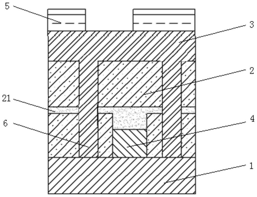
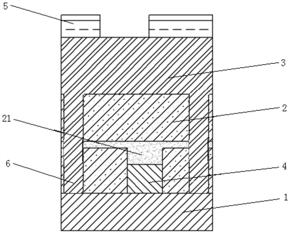
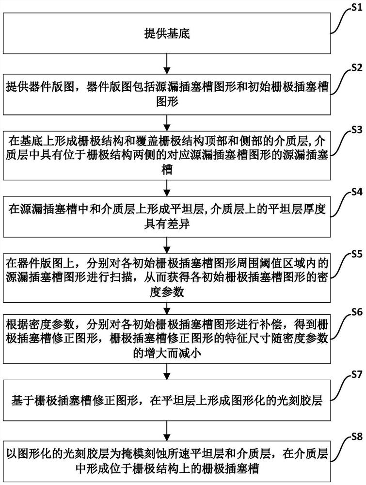
[0063] The implementation of the present invention will be illustrated by specific specific examples below, and those skilled in the art can easily understand other advantages and effects of the present invention from the content disclosed in this specification. Although the description of the present invention will be presented in conjunction with a preferred embodiment, it does not mean that the features of the invention are limited to this embodiment. On the contrary, the purpose of introducing the invention in conjunction with the embodiments is to cover other options or modifications that may be extended based on the claims of the present invention. The following description contains numerous specific details in order to provide a thorough understanding of the present invention. The invention may also be practiced without these details. Also, some specific details will be omitted from the description in order to avoid obscuring or obscuring the gist of the present invent...


PUM


Abstract

The invention discloses a formation method of a semiconductor device, wherein the method comprises the steps: providing a device layout, and respectively scanning source and drain plug groove patterns in a threshold region around each initial gate plug groove pattern so as to obtain a density parameter of each initial gate plug groove pattern; according to the density parameter, each initial gate plug groove pattern is compensated to obtain a gate plug groove correction pattern, and the feature size of the gate plug groove correction pattern is reduced along with the increase of the density parameter; and a flat layer and a dielectric layer are etched to form a gate plug groove. By adopting the scheme, the rates of etching the dielectric layer and the flat layer are relatively low in the region with relatively high density of the source and drain plug groove, so that the problem of over-etching when the gate plug groove is formed by etching is avoided. In the region with the small density of the source and drain plug groove, the rate of etching the dielectric layer and the flat layer is large, and the problem that etching is insufficient when the gate plug groove is formed through etching is avoided. Therefore, the morphology of the finally formed gate plug groove is more uniform.

Description

technical field [0001] The invention relates to the technical field of semiconductors, in particular to a method for forming a semiconductor device. Background technique [0002] In the semiconductor manufacturing process, it is a very important and complicated process to transfer the pattern on the mask to the semiconductor chip through the steps of photolithography and etching. [0003] The size of a specific pattern after photolithography is characterized by the after develop inspection critical dimension (ADI CD), and the size of the ADI CD directly affects the after Etch inspection critical dimension (AEI CD) . Before etching, it is necessary to deposit a dielectric layer and a planar layer, and form a patterned photoresist layer on the planar layer, and then use the patterned photoresist layer to etch the planar layer and then the dielectric layer. [0004] The density of the source-drain plug grooves formed in the dielectric layer under the flat layer is different, ...

Claims


Application Information

Patent Timeline
IPC IPC(8): H01L21/336H01L29/423H01L21/027H01L21/311
CPCH01L29/66477H01L29/42356H01L21/0274H01L21/31144
Inventor 钱亚峰张婉娟朱占魁李晓波
Owner SEMICON MFG INT (SHANGHAI) CORP
Why Eureka
Try Eureka