Fault positioning method and fault positioning device

A fault location and fault location technology, applied in short-circuit testing, optical testing flaws/defects, electrical radiation detectors, etc., can solve the problems of location failure, high failure rate, missed leakage points, etc. Sample structure, the effect of shortening positioning time

Pending Publication Date: 2021-10-01
深圳市美信咨询有限公司
View PDF0 Cites 5 Cited by
  • Summary
  • Abstract
  • Description
  • Claims
  • Application Information

AI Technical Summary

Problems solved by technology

[0004] The above two methods are very blind. Since the leakage position of the IC carrier board is completely unpredictable, the grinding process is random, which takes a long time and is inefficient; and because the leakage position of the IC carrier board is located in its internal The dielectric layer, the leakage area is small (especially in the case of small leakage), the leakage position is easily ground off during the grinding process, and the leakage point is missed, resulting in a complete failure of positioning, so the failure rate is extremely high

Method used


Image

  • Fault positioning method and fault positioning device
  • Fault positioning method and fault positioning device
  • Fault positioning method and fault positioning device

Examples


Embodiment 1

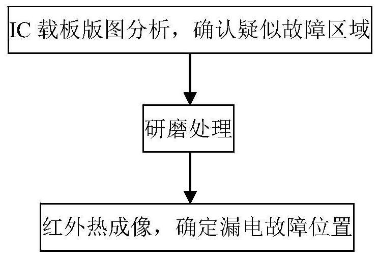
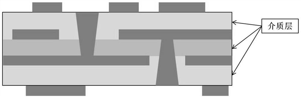
[0084] Such as figure 1 As shown, this embodiment provides an IC carrier board ( figure 2 It is the structural schematic diagram of the IC carrier board) the positioning method of the leakage fault position, specifically including:

[0085] 1. Use impedance testing equipment to perform impedance test on the faulty IC carrier board, and record the abnormal impedance value (impedance ≤ 10 8 Ω).

[0086] During the test, the magnitude of the leakage current is controlled, and it is controlled at the μA level to minimize the secondary damage of the current.

[0087] 2. Use the layout of the IC carrier board to conduct impedance tests on the lines that may have problems one by one, and continuously narrow the scope until the smallest suspected fault area is determined, such as confirming which layer the suspected fault area is on the carrier board, and which lines are in between Wait.

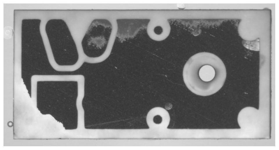
[0088] 3. Carry out plane grinding for the suspected faulty area identified on the IC carri...

Embodiment 2

[0096] This embodiment provides a method for locating the location of an IC carrier board leakage fault, which specifically includes:

[0097] 1. Use impedance testing equipment to perform impedance test on the faulty IC carrier board, and record the abnormal impedance value (impedance ≤ 10 8 Ω).

[0098] During the test, the magnitude of the leakage current is controlled, and it is controlled at the μA level to minimize the secondary damage of the current.

[0099] 2. Use the layout of the IC carrier board to conduct impedance tests on the lines that may have problems one by one, and continuously narrow the scope until the smallest suspected fault area is determined, such as confirming which layer the suspected fault area is on the carrier board, and which lines are in between Wait.

[0100] 3. Carry out plane grinding for the suspected faulty area identified on the IC carrier board. The grinding method is ordinary mechanical grinding. First, use coarse sandpaper to grind, ...

Embodiment 3

[0106] This embodiment provides a method for locating the location of an IC carrier board leakage fault, which specifically includes:

[0107] 1. Use impedance testing equipment to perform impedance test on the faulty IC carrier board, and record the abnormal impedance value (impedance ≤ 10 8Ω).

[0108] During the test, the magnitude of the leakage current is controlled, and it is controlled at the μA level to minimize the secondary damage of the current.

[0109] 2. Use the layout of the IC carrier board to conduct impedance tests on the lines that may have problems one by one, and continuously narrow the scope until the smallest suspected fault area is determined, such as confirming which layer the suspected fault area is on the carrier board, and which lines are in between Wait.

[0110] 3. Carry out plane grinding for the suspected faulty area identified on the IC carrier board. The grinding method is ordinary mechanical grinding. First, use coarse sandpaper to grind, a...


PUM

PropertyMeasurementUnit
impedanceaaaaaaaaaa

Abstract

The invention provides a fault positioning method and a fault positioning device, and relates to the field of semiconductors. The fault positioning method comprises the following steps: pre-judging a suspected fault area by using the layout of the fault IC carrier plate and an impedance test result, and then grinding the suspected fault area; and electrifying the ground fault IC carrier plate, carrying out thermal imaging on the electrified fault IC carrier plate, and obtaining a temperature abnormal area, wherein the temperature abnormal area is a leakage fault position. The fault positioning device comprises an impedance detection module, a grinding module, a power supply module and an infrared imaging module, the impedance detection module is used for detecting the impedance of the fault IC carrier plate, the grinding module is used for grinding a suspected fault area of the fault IC carrier plate, and the power supply module is used for electrifying the ground fault IC carrier plate. And the infrared imaging module is used for carrying out thermal imaging on the electrified fault IC carrier plate. The fault positioning method and the fault positioning device provided by the invention are accurate in positioning, high in success rate and short in time consumption.

Description

technical field [0001] The present application relates to the field of semiconductors, and in particular to a fault location method and a fault location device. Background technique [0002] IC substrate is a key special basic material for integrated circuit packaging, which mainly protects the chip and acts as an interface between the integrated circuit chip and the outside world. The structure of high-precision IC substrate is relatively simple, and its inherent feature is that the insulating dielectric layer is extremely thin, so the typical failure mode is local leakage and insufficient withstand voltage. [0003] At present, there are two mainstream positioning methods in the industry, one is section grinding and the other is plane grinding. The cross-section grinding method mainly includes: potting and curing the faulty IC carrier board, and the potting material is epoxy resin; mechanically grinding the cured faulty sample perpendicular to the board surface, and mecha...

Claims


Application Information

Patent Timeline
Patent Type & Authority Applications(China)
IPC IPC(8): G01R31/52G01J5/10G01N21/88
CPCG01R31/52G01J5/10G01N21/88
Inventor 王君兆黄伟
Owner 深圳市美信咨询有限公司
Why Eureka
Try Eureka