Heterosynaptic electronic device based on two-dimensional ferroelectric semiconductor and preparation method of heterosynaptic electronic device

An electronic device and semiconductor technology, applied in the field of heterologous synaptic electronic devices and their preparation, can solve problems such as difficulty in simulating heterologous synaptic plasticity, and achieve the effects of reducing operating voltage and avoiding air oxidation

Pending Publication Date: 2021-10-12
UNIV OF ELECTRONICS SCI & TECH OF CHINA
View PDF1 Cites 5 Cited by
  • Summary
  • Abstract
  • Description
  • Claims
  • Application Information

AI Technical Summary

Problems solved by technology

[0005] The purpose of the present invention is to provide a heterosynaptic electronic device based on a two-dimensional ferroelectric semiconductor and its preparation method for the technical problem that the existing artificial synaptic electronic devices are difficult to simulate the plasticity of heterogeneous synapses. 2 -VI 3 Two-dimensional ferroelectric semiconductor material is a memristive transistor with a conductive channel, which realizes the control of synaptic weight by inputting from both ends of the source, drain and gate

Method used


Image

  • Heterosynaptic electronic device based on two-dimensional ferroelectric semiconductor and preparation method of heterosynaptic electronic device
  • Heterosynaptic electronic device based on two-dimensional ferroelectric semiconductor and preparation method of heterosynaptic electronic device
  • Heterosynaptic electronic device based on two-dimensional ferroelectric semiconductor and preparation method of heterosynaptic electronic device

Examples


Embodiment 1

[0041] A preferred embodiment of the present invention provides a method for preparing a heterosynaptic electronic device based on a two-dimensional ferroelectric semiconductor. The specific steps are as follows:

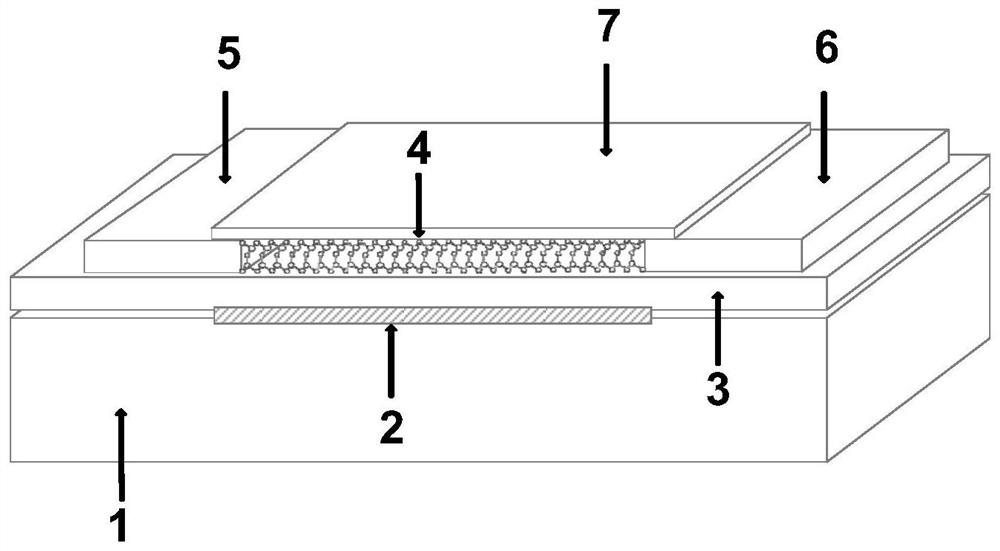
[0042] 1) On SiO 2 A metal Au electrode was prepared on the substrate: first, the heavily doped Si / SiO 2 Strip mask patterns with 5 μm intervals and 10 μm width were etched on the substrate, and then thermal evaporation coating equipment was used to A 50nm-thick Au film was deposited on the substrate at a rate of 50nm, and then the substrate was immersed in an acetone solution for 30min and then lifted-off to obtain a patterned Au electrode.

[0043] 2) Preparation of PVA dry transfer film: first prepare a 10wt% PVA aqueous solution, and then take 5mL of the solution and drop it on the cleaned SiO 2 The substrate is then placed on a heating plate at a temperature of 50°C and baked for 10 minutes to obtain a PVA film; then a blade cuts a 3mm×3mm PVA film and place...

Embodiment 2

[0048] A preferred embodiment of the present invention provides a method for preparing a heterosynaptic electronic device based on a two-dimensional ferroelectric semiconductor. The specific steps are as follows:

[0049] 1) Preparation of encapsulation layer h-BN and graphene electrode: choose Si / SiO 2 As a supporting substrate, use mechanical exfoliation to obtain few-layer h-BN samples from h-BN crystals, and obtain single-layer or few-layer graphene samples from graphite layered crystals. location marker.

[0050] 2) Preparation of PVA dry transfer film: first prepare a 10wt% PVA aqueous solution, and then take 5mL of the solution and drop it on the cleaned SiO 2 Substrate, then place it on a heating plate at a temperature of 50°C and bake for 1 hour to obtain a PVA film; then a blade cuts out a PVA film with a size of about 3mm×3mm, and places it on a transparent glass sheet with the flat side facing up. On the PDMS substrate, finally obtain the PVA dry transfer film. ...

Embodiment 3

[0055] 1) On SiO 2 Metallic Pt electrodes prepared on the substrate: on Si / SiO 2 The substrate self-assembles a layer of monomolecular film, and a hard metal mask plate containing electrode patterns with a spacing width of 7um is placed on the substrate, and then thermal evaporation coating equipment is used to A 50nm-thick Pt film was deposited on the substrate at a rate of 50 nm, and a patterned Pt electrode was obtained by removing the metal mask.

[0056] 2) Preparation of PVA dry transfer film: first prepare a 10wt% PVA aqueous solution, and then take 5mL of the solution and drop it on the cleaned SiO 2 The substrate is then placed on a heating plate at a temperature of 50°C and baked for 10 minutes to obtain a PVA film; then a blade cuts a 3mm×3mm PVA film and places it on a PDMS substrate of the same size adhered to one end of a transparent glass sheet. Thus a PVA dry transfer film was obtained.

[0057] 3) PVA dry transfer of Pt electrodes: With the aid of a micros...


PUM


Abstract

The invention discloses a heterosynapse electronic device based on a two-dimensional ferroelectric semiconductor and a preparation method of the heterosynapse electronic device. The heterosynapse electronic device comprises a supporting substrate, a back gate electrode, a dielectric layer, a source-drain electrode and a packaging layer which are sequentially stacked from bottom to top, the source and drain electrode comprises a source electrode and a drain electrode, a conducting channel is arranged between the source electrode and the drain electrode, and the conducting channel is made of a III2-VI3 type two-dimensional ferroelectric semiconductor material; the source electrode and the drain electrode are respectively connected with two ends of the conducting channel and form Schottky contact with a Van der Waals interface; and the preparation method comprises the steps of preparing the packaging layer h-BN and the graphene electrode, preparing a PVA dry-method transfer film, performing dry-method transfer on the graphene electrode, preparing the graphene source and drain electrode and preparing the metal extraction electrode. The invention provides a memristive transistor which takes a III2-VI3 two-dimensional ferroelectric semiconductor material as a conducting channel, and realizes a heterosynaptic electronic device for regulating and controlling synaptic weight by inputting from two ends of a source electrode, a drain electrode and a grid electrode.

Description

technical field [0001] The invention belongs to the technical field of semiconductors and novel non-von Neumann computing, and specifically relates to a heterogeneous synaptic electronic device based on a two-dimensional ferroelectric semiconductor and a preparation method thereof. Background technique [0002] The electronic computer with the traditional complementary metal-insulator-semiconductor (CMOS) as the core device of the integrated circuit has realized technological innovation in many fields and led us into the modern information society. However, due to the separation of memory and processor, traditional computers face a serious "memory wall" problem when processing large-scale data. Researchers address the dilemmas faced by artificial intelligence algorithms such as neural networks and deep learning as they optimize computers to process large amounts of data. However, limited by the requirements of the hardware environment in which the software and algorithms th...

Claims


Application Information

Patent Timeline
Patent Type & Authority Applications(China)
IPC IPC(8): H01L27/1159
CPCH10B51/30
Inventor 刘富才曹桂铭陈建钢蒙鹏刘海石
Owner UNIV OF ELECTRONICS SCI & TECH OF CHINA
Why Eureka
Try Eureka