
Material surface fog detection method and device

A detection material and signal detection technology, which is applied in measurement devices, analysis materials, and optical devices, etc., can solve problems such as inability to detect, lack of accurate detection materials, and no reference significance, and achieve the effect of accurate detection.

Active Publication Date: 2021-10-15
BEIJING TONGMEI XTAL TECH CO LTD
View PDF8 Cites 3 Cited by
  • Summary
  • Abstract
  • Description
  • Claims
  • Application Information

AI Technical Summary

Problems solved by technology

[0018] However, there is currently no effective method for accurately detecting surface fog on materials (such as wafers, especially compound semiconductor wafers) in the art
[0019] CN111272773A discloses a high-resolution detection system for semiconductor wafer surface defects, which is based on a defect detection method and equipment for frequency-shifted lighting. However, it is for the detection of semiconductor surface particles and does not involve the detection of surface fog
However, due to the presence of the photoluminescence signal, both the measured surface fog distribution and values ​​may be higher than the real situation of the material surface, or, the real situation of the surface fog (especially in the case of low surface fog) may be Masked by photoluminescent signal and cannot be detected - in these cases, the results obtained by surface fog detection are actually "false" results, and what's more, the material under test may be due to such "false" results It was judged as unqualified, so these test results have no reference significance in quality control of materials
Moreover, such test results are meaningless when traced back to the problematic production link.

Method used


Image

  • Material surface fog detection method and device
  • Material surface fog detection method and device
  • Material surface fog detection method and device

Examples


Embodiment 1

[0139] Surface haze inspection on 3-inch N-type InP (sulfur-doped) wafers. Carry out the following steps to the wafer after cleaning and drying:

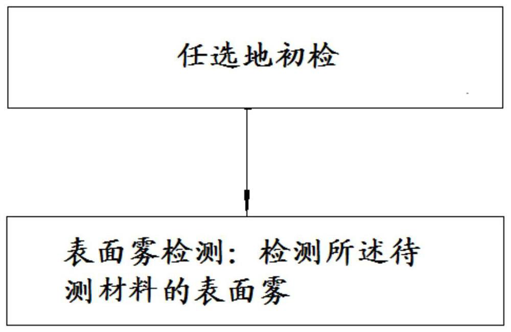
[0140] 1. Initial inspection. The cleaned wafers are inspected with the strong light of Japan Yamada Optical. Adjust the illumination to not less than 400,000lx. During the lamp inspection, under the strong light, slowly rotate the wafer one circle clockwise, then slowly rotate the wafer counterclockwise for one circle, carefully observe to check whether there are visually visible defects on the wafer surface (such as scratches, potion residue, orange peel type, etc.) defect). After the wafer is confirmed to have no visual defects by light inspection, it is qualified for the initial inspection. Wafers that pass the initial inspection are used for surface fog testing.

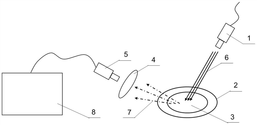
[0141] 2. Surface fog detection. The detection equipment uses the Lightspeed equipment of the 4See series of the French Unity SC company.

[0142] a. Put the w...

Embodiment 2

[0151] Surface haze inspection on 3-inch N-type InP (sulfur-doped) wafers. Carry out the following steps to the wafer after cleaning and drying:

[0152] 1. Initial inspection. The cleaned wafers are inspected with the strong light of Japan Yamada Optical. Adjust the illumination to not less than 400,000lx. The light inspection method and qualification criteria are the same as those in Example 1. Wafers that pass the initial inspection are used for surface fog testing.

[0153] 2. Surface fog detection. The detection equipment uses the Lightspeed equipment of the 4See series of the French Unity SC company.

[0154] a. Put the wafers that pass the preliminary inspection into the testing equipment and place them in the wafer loading device (wafer chuck). A blue laser with a wavelength of 473nm is used as the incident light.

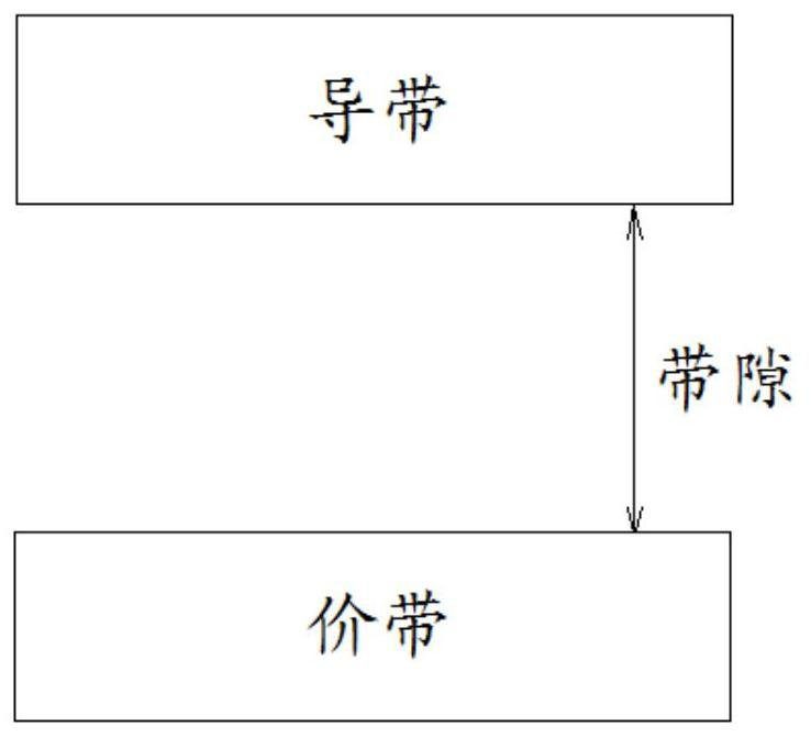
[0155] b. Select the optical filter module. Since the wafer to be tested is an InP material with a band gap of 1.35eV, the photoluminescent wavelen...

Embodiment 3

[0163] Surface fog inspection on 3-inch Un-type InP (non-doped) wafers. Carry out the following steps to the wafer after cleaning:

[0164] 1. Initial inspection. The cleaned wafers are inspected with the strong light of Japan Yamada Optical. Adjust the illumination to not less than 400,000lx. The light inspection method and qualification criteria are the same as those in Example 1. Wafers that pass the initial inspection are used for surface fog testing.

[0165] 2. Surface fog detection. The detection equipment uses the Lightspeed equipment of the 4See series of the French Unity SC company.

[0166] a. Put the wafers that pass the preliminary inspection into the testing equipment and place them in the wafer loading device (wafer chuck). A blue laser with a wavelength of 473nm is used as the incident light.

[0167] b. Select the optical filter module. Since the wafer to be tested is an InP material with a band gap of 1.35eV, the photoluminescent wavelength of the mat...


PUM

PropertyMeasurementUnit
band gapaaaaaaaaaa
band gapaaaaaaaaaa
wavelengthaaaaaaaaaa

Abstract

The invention provides a material surface fog detection method, which comprises the following steps of: optionally performing initial detection: performing initial detection on the material to obtain a material without visual defects on the surface; and performing surface fog detection: detecting the surface fog of the material, wherein in the surface fog detection equipment, a photoluminescence signal of a material is filtered out through an optical filter module in a receiving light path, so that the photoluminescence signal is not detected by a detector. The invention further provides a device for detecting the material surface fog. According to the method and the device for detecting the surface fog, an unexpected material photoluminescence signal is filtered out, so that a material surface fog detection result can be more accurately obtained.

Description

technical field [0001] The invention relates to the field of material detection. More specifically, the present invention relates to a method and device for detecting material surface, and more particularly, to a method and device for detecting fog on material surface. Background technique [0002] With the development of science and technology, in some fields, the requirements for the surface finish of materials (such as semiconductor wafers, glass or ceramics) are getting higher and higher. For example, in the fields of electronics, communication, etc., the requirements for the surface of semiconductor wafers are increasing day by day. Since the birth of electronic components in the 1950s, semiconductor materials have been widely used in modern production and life, and their importance is self-evident. With the development of semiconductor devices toward miniaturization and integration, the influence of the surface state of the substrate on device characteristics is beco...

Claims


Application Information

Patent Timeline
Patent Type & Authority Applications(China)
IPC IPC(8): G01B11/30
CPCG01B11/30G01N21/9501
Inventor 高伟刘宇王志珍李海淼
Owner BEIJING TONGMEI XTAL TECH CO LTD
Learn More