
Composite window structure for improving heat resistance of microwave CVD window
A technology of heat resistance and microwave, applied in the improvement of windows/doors, metal material coating process, coating, etc., can solve the problems of loss of vacuum seal, heat damage, damage, etc., to avoid overheating and increase power value Effect
- Summary
- Abstract
- Description
- Claims
- Application Information
AI Technical Summary
Problems solved by technology
Method used
Image

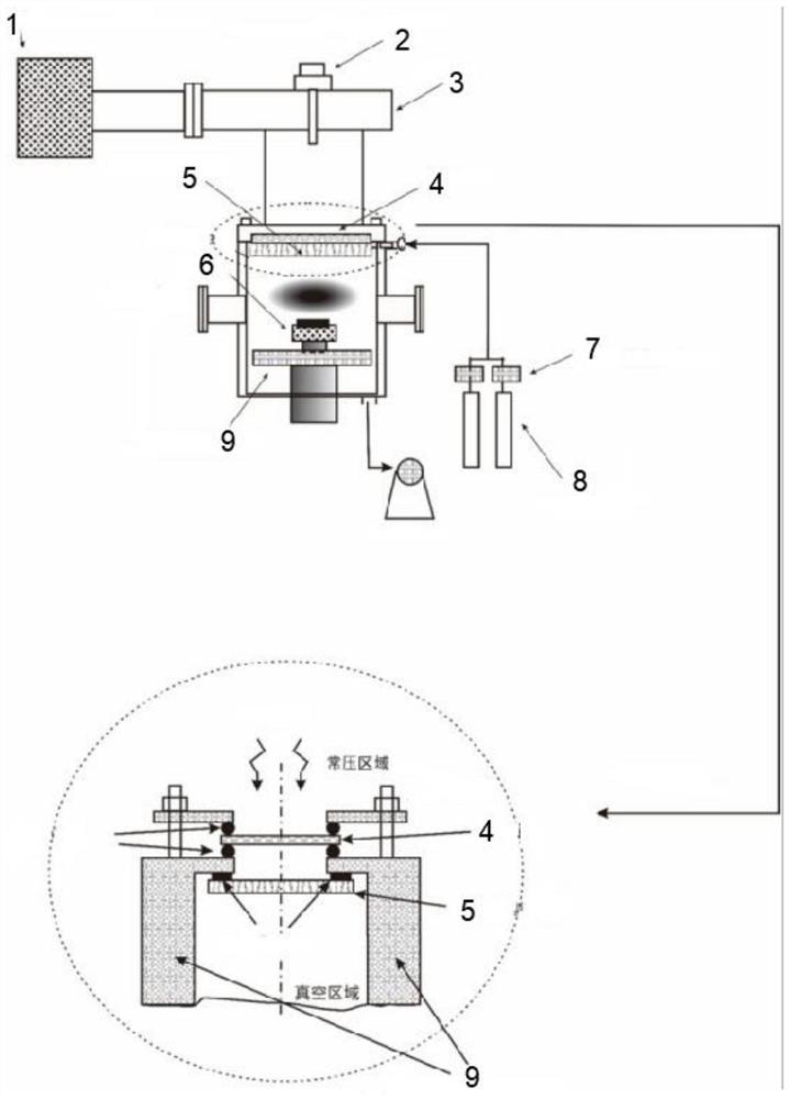
Examples
Embodiment 1
[0027] The material of the microwave window on the upper layer is silicon dioxide, the thickness: 10.0mm; there is no microwave window on the lower layer.
[0028] The microwave input power is 5KW, the pressure in the metal vacuum chamber is 21.0kPa, the gas flow rate is H2:CH4=200:4.0sccm (sccm: standard cubic centimeter per minute), the growth temperature of CVD diamond film is 880°C, and the substrate material is single crystal silicon piece. After working for 8 hours, the thickness of the CVD diamond film was measured, and the calculated growth rate was 6.2 μm / hour: the content of Si in the CVD diamond film was 1.153 ppm through secondary mass spectrometry analysis.
Embodiment 2
[0030] The material of the upper microwave window is silicon dioxide, the thickness is 10.0mm; the lower microwave window is set under it.
[0031] The material of the microwave window in the lower layer is two CVD diamond, the thickness is 1.5 mm; the brazing width of the outer edge is 3.0 mm.
[0032] The microwave input power is 10KW, the pressure in the metal vacuum chamber is 21.0kPa, the gas flow rate is H2:CH4=200:4.0sccm (sccm: standard cubic centimeter per minute), the growth temperature of CVD diamond film is 880°C, and the substrate material is single crystal silicon piece. After working for 8 hours, the thickness of the CVD diamond film was measured, and the growth rate was calculated to be 8.6 μm / hour: the content of Si in the CVD diamond film was 0.218 ppm through secondary mass spectrometry analysis.
[0033] Comparing Example 1 and Example 2, it can be concluded that due to the use of the composite microwave window, the etching effect of the plasma ball on the...
PUM
| Property | Measurement | Unit |
|---|---|---|
| thickness | aaaaa | aaaaa |
| thickness | aaaaa | aaaaa |
| thickness | aaaaa | aaaaa |
Abstract
Description
Claims
Application Information